***edit*** some ppl think the range for flops is now 176-450. it depends on the number of ALU's per SIMD unit.
Some people at Neogaf got some die pics of the WiiU GPU, and it turns out that its crazy customized. It barely resembles an r700. Some people estimate that the floating point performance for the programmable shaders is around 176. In comparison Xenos is 240. The question everyone has is how the WiiU manages to run the games from teh current gen consoles with such a difference. Obviously flops cant be directly compared, but 176 is still a low number(an order of maginitude different). The idea is that the WiiU's fixed function hardware is what is allowing the console to be so energy efficient, and slightly outperform the current gen systems. Before anyone calls Nintendo cheap keep in mind custom hardware is more expensive than going the traditional route lie slightly modifying an off the shelf gpu which is what Sony and Microsoft tend to do. I guess you really can say that the WiiU is another gamecube. Personally i think its an amazing feat of engineering, and one of the reasons i like Nintendo. They do weird and cool stuff, and while it may not benefit gamers it certainly is interesting for those who are more interested in this kind of stuff.
Here is teh thread:
http://www.neogaf.com/forum/showthread.php?t=511628
What's going on here?
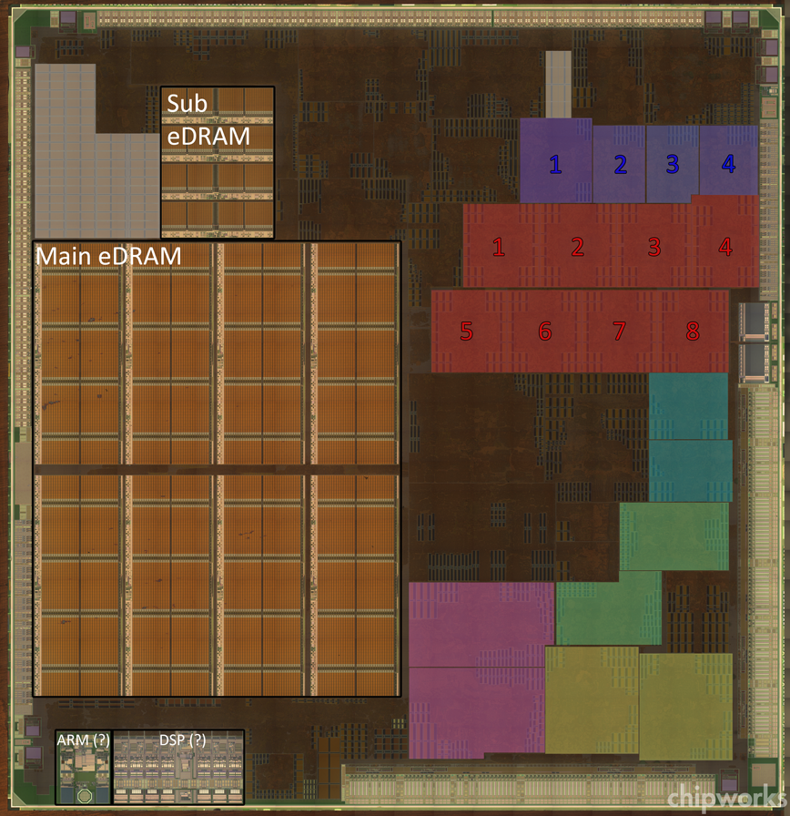
A few days ago, wsippel noticed that Chipworks had Wii U die photos up for sale on their website, and at $200 a piece (for each of the CPU, GPU and NOR dies), some of us in the Wii U Technical Discussion Thread decided to chip in a few dollars each to buy the GPU photo, with the aim of a few of us (Fourth Storm, wsippel, Blu, Durante and myself) deciphering it and posting up our results on GAF. Chipworks, though, decided to be amazingly kind and helpful, and sent an email back to us offering not only to do a higher quality polysilicon die photo for us at their expense (as they felt their existing shot didn't give us the detail we needed), but to allow us to post the full-res photo up here on GAF for all you lovely folks to enjoy!
We had originally planned on taking a day or so to figure the chip out before posting this, but as Chipworks already put it up on their blog, we figured might as well just throw this up and do the analysis in real-time.
What am I looking at?
Well, the first thing to note is that we're looking at something very different from a standard R700 die (we know that Latte is based on AMD's R700 line originally). This makes it more difficult than we'd hoped to analyse, as comparison to existing AMD die shots would generally be our main strategy. There are a few things we can say so far, though:
- The die is exactly 11.88 x 12.33mm (146.48mm²)
- The large orange block on the left is the 32MB of eDRAM (MEM1).
- The smaller orange block above it seems to be about 3MB of eDRAM. This might be the framebuffer for Wii mode, or the L2 texture cache, or something else, we're not 100% sure at this point.
- In the lower left there is what appears to be a dual-core ARM (used for security/streaming purposes) and possibly a DSP (or custom logic for the video streaming).
- Along the bottom and right sides of the chip are likely DDR3 controllers. The top and left sides of the chip are probably for communication with the CPU.
- All the small dark orange/black blocks you see over the GPU part of the die are SRAM blocks. The number and formation of them should give us clues as to what part of the chip does what.
- The eight squarish groupings on the right hand side are possibly the VLIW5 shader clusters. However, due to the apparent increased amount of SRAM there, along with the unusual layout and the general changes to the die, it's entirely possible that the number of shaders in each cluster has changed from R700 dies. In fact, at this point it's even possible that the microarchitecture itself has changed, a la the VLIW4 used in some of AMD's 6000 series GPUs. Therefore, we could have a fairly unusual number of shader cores.
- It's likely there's some legacy Broadway hardware on there for BC purposes.
Up: To clarify, Wii's "Broadway" GPU (inc. eDRAM) was 8mm x 9mm, or 72mm² on a 90nm process. That would only account for about 10-20% of the die space on a 146.48mm² 40nm chip, if they just slapped Broadway on there. However, given Shiota's comment here, many of the Wii BC functions should actually be handled by the Wii U's GPU hardware, so the actual amount of die space used purely for Wii BC should be very small, possibly just 5-10%.
I'll be updating this post as more info is figured out, so check back for updates.Red are the (presumed) shader clusters. Blue are the (presumed) TMUs.
The rest of the colorization are simply self-similar components that may not be layed down exactly in square blocks, but are still recognizable.
Neogaf dude


 Wii U version:
  Nintendo will finally purify the corrupted minds and bring back true gaming quality. The Vita will also help in this. With over 4 million sold world wide, the Wii U is unstoppable with breaking bone speeds.


Log in to comment