Digital Foundry: PS5 & Next Xbox Speculative Power

  • 116 results
  • 1
  • 2
  • 3
Avatar image for ronvalencia
ronvalencia

29612

Forum Posts

0

Wiki Points

0

Followers

Reviews: 1

User Lists: 0

#51  Edited By ronvalencia
Member since 2008 • 29612 Posts

@scatteh316 said:
@Grey_Eyed_Elf said:
@scatteh316 said:
@Grey_Eyed_Elf said:

Its because GCN hit its limit of 64 CU's and Navi is GCN based.. Its why DF focused on it as well, AMD's tflop's are based on multiplying the CU count of the chip by 64.

If the PS5 was using AMD's Next Gen architecture then we wouldn't know a thing, but knowing that its using GCN based Navi which tops out at 64 CU's there's really no other thing to focus on other than core clocks and CU's because those two specifications are what is used to give the chips tflop count with GCN.

But with knowing how bottlenecked the CU's are on current chips they can get massive gains without even touching the CU's...... and we don't know what they're doing to the rest of the chip.

They need to start increasing the ratio of CU:ROP/TMU before they even think about total CU count.

They could do just that and like DF mentioned they could increase the die size to boost the CU count also but the problem with doing either of those is time and money, you would need several months of RND in order to just design such a custom chip and then to mass produce them would cost even more.

.

Adding more ROPs and TMU's would not be a custom solution for the consoles, it's something AMD need to starting doing for their whole product lineup.

Thus it should filter down to the console's SOC naturally.

290x = 64 ROPS

Fury X = 64 ROPS

Vega 64 = 64 ROPS

780ti = 48 ROPS

980ti = 96 ROPS

1080ti = 96 ROPS

AMD need to make massive changes to their architecture.

Running Vega 56 and Vega 64 at the same clock speeds show's no additional performance for Vega 64 despite the extra CU's as the ROPS/TMU's are holding the shader cores back.

Simply bumping up the CU count in a next generation console SOC won't be as effective as it should be if they don't fix the un-balanced nature of the chip along side it.

290X = 64 ROPS non-tile cache architecture

Fury X = 64 ROPS non-tile cache architecture with lower latency external memory.

Vega 64 = 64 ROPS at 1500 Mhz tile cache architecture. 4 MB L2 cache. Unknown if Polaris delta compression is applied at this memory level.

----------

780 Ti = 48 ROPS non-tile cache architecture.

980 Ti = 96 ROPS at 1076 Mhz tile cache architecture. ~3 MB L2 cache with Maxwell delta compression

1080 = 64 ROPS at ~1800 Mhz tile cache architecture. ~2 MB L2 cache with better Pascal delta compression

1080 Ti = 88 ROPS at ~1800 Mhz tile cache architecture. ~3 MB L2 cache with better Pascal delta compression. 1080 Ti's L2 cache (>1 TB/s) performance is superior to 980 Ti's L2 cache (~600 GB/s)

Titan XP = 96 ROPS tile cache architecture

AMD needs to lower CU count and increase clock speed e.g. GTX 1080 is like 40 CU GCN with ~1800Mhz clock speed (64 ROPS scaled with is clock speed)

Vega 56/64 extra CUs are wasting power. AMD should have 44 CU setup 64 ROPS and spend extra TDP headroom for higher clock speed.
Avatar image for scatteh316
scatteh316

10273

Forum Posts

0

Wiki Points

0

Followers

Reviews: 0

User Lists: 0

#52 scatteh316
Member since 2004 • 10273 Posts

@ronvalencia said:
@scatteh316 said:
@Grey_Eyed_Elf said:
@scatteh316 said:
@Grey_Eyed_Elf said:

Its because GCN hit its limit of 64 CU's and Navi is GCN based.. Its why DF focused on it as well, AMD's tflop's are based on multiplying the CU count of the chip by 64.

If the PS5 was using AMD's Next Gen architecture then we wouldn't know a thing, but knowing that its using GCN based Navi which tops out at 64 CU's there's really no other thing to focus on other than core clocks and CU's because those two specifications are what is used to give the chips tflop count with GCN.

But with knowing how bottlenecked the CU's are on current chips they can get massive gains without even touching the CU's...... and we don't know what they're doing to the rest of the chip.

They need to start increasing the ratio of CU:ROP/TMU before they even think about total CU count.

They could do just that and like DF mentioned they could increase the die size to boost the CU count also but the problem with doing either of those is time and money, you would need several months of RND in order to just design such a custom chip and then to mass produce them would cost even more.

.

Adding more ROPs and TMU's would not be a custom solution for the consoles, it's something AMD need to starting doing for their whole product lineup.

Thus it should filter down to the console's SOC naturally.

290x = 64 ROPS

Fury X = 64 ROPS

Vega 64 = 64 ROPS

780ti = 48 ROPS

980ti = 96 ROPS

1080ti = 96 ROPS

AMD need to make massive changes to their architecture.

Running Vega 56 and Vega 64 at the same clock speeds show's no additional performance for Vega 64 despite the extra CU's as the ROPS/TMU's are holding the shader cores back.

Simply bumping up the CU count in a next generation console SOC won't be as effective as it should be if they don't fix the un-balanced nature of the chip along side it.

And you've replied to me because????

Avatar image for Grey_Eyed_Elf
Grey_Eyed_Elf

7970

Forum Posts

0

Wiki Points

0

Followers

Reviews: 0

User Lists: 0

#53 Grey_Eyed_Elf
Member since 2011 • 7970 Posts

@scatteh316: He is pointing out that not all ROPS are equal similar to TFLOP counts.

Avatar image for ronvalencia
ronvalencia

29612

Forum Posts

0

Wiki Points

0

Followers

Reviews: 1

User Lists: 0

#54 ronvalencia
Member since 2008 • 29612 Posts

@scatteh316 said:
@ronvalencia said:
@scatteh316 said:
@Grey_Eyed_Elf said:
@scatteh316 said:

But with knowing how bottlenecked the CU's are on current chips they can get massive gains without even touching the CU's...... and we don't know what they're doing to the rest of the chip.

They need to start increasing the ratio of CU:ROP/TMU before they even think about total CU count.

They could do just that and like DF mentioned they could increase the die size to boost the CU count also but the problem with doing either of those is time and money, you would need several months of RND in order to just design such a custom chip and then to mass produce them would cost even more.

.

Adding more ROPs and TMU's would not be a custom solution for the consoles, it's something AMD need to starting doing for their whole product lineup.

Thus it should filter down to the console's SOC naturally.

290x = 64 ROPS

Fury X = 64 ROPS

Vega 64 = 64 ROPS

780ti = 48 ROPS

980ti = 96 ROPS

1080ti = 96 ROPS

AMD need to make massive changes to their architecture.

Running Vega 56 and Vega 64 at the same clock speeds show's no additional performance for Vega 64 despite the extra CU's as the ROPS/TMU's are holding the shader cores back.

Simply bumping up the CU count in a next generation console SOC won't be as effective as it should be if they don't fix the un-balanced nature of the chip along side it.

And you've replied to me because????

Your's ROPS list is not complete since there was a shift from non-tile cache architecture to tile cache architecture. ROPS are not built equally.

Avatar image for Grey_Eyed_Elf
Grey_Eyed_Elf

7970

Forum Posts

0

Wiki Points

0

Followers

Reviews: 0

User Lists: 0

#55 Grey_Eyed_Elf
Member since 2011 • 7970 Posts

@ronvalencia said:

AMD needs to lower CU count and increase clock speed e.g. GTX 1080 is like 40 CU GCN with ~1800Mhz clock speed (64 ROPS scaled with is clock speed)

Vega 56/64 extra CUs are wasting power. AMD should have 44 CU setup 64 ROPS and spend extra TDP headroom for higher clock speed.
I fully agree with you that this would be a great viable path in the desktop segment, but for a console the main issue at that point would be heat dissipation. We all know that consoles are known for saving money on just that.

AMD has a similar issue with Zen, its clocked almost 200-400MHz lower than the equivalent Intel counterpart with the additional per core performance advantage it completely destroys Ryzen for gaming.

I don't know what AMD is doing to be honest they seem to take one step forward then 2 steps back lately.

Avatar image for scatteh316
scatteh316

10273

Forum Posts

0

Wiki Points

0

Followers

Reviews: 0

User Lists: 0

#56 scatteh316
Member since 2004 • 10273 Posts

@Grey_Eyed_Elf said:

@scatteh316: He is pointing out that not all ROPS are equal similar to TFLOP counts.

Yes I know that but it wasn't relevant to my point.

Avatar image for scatteh316
scatteh316

10273

Forum Posts

0

Wiki Points

0

Followers

Reviews: 0

User Lists: 0

#57 scatteh316
Member since 2004 • 10273 Posts

@ronvalencia said:
@scatteh316 said:
@ronvalencia said:
@scatteh316 said:
@Grey_Eyed_Elf said:

They could do just that and like DF mentioned they could increase the die size to boost the CU count also but the problem with doing either of those is time and money, you would need several months of RND in order to just design such a custom chip and then to mass produce them would cost even more.

.

Adding more ROPs and TMU's would not be a custom solution for the consoles, it's something AMD need to starting doing for their whole product lineup.

Thus it should filter down to the console's SOC naturally.

290x = 64 ROPS

Fury X = 64 ROPS

Vega 64 = 64 ROPS

780ti = 48 ROPS

980ti = 96 ROPS

1080ti = 96 ROPS

AMD need to make massive changes to their architecture.

Running Vega 56 and Vega 64 at the same clock speeds show's no additional performance for Vega 64 despite the extra CU's as the ROPS/TMU's are holding the shader cores back.

Simply bumping up the CU count in a next generation console SOC won't be as effective as it should be if they don't fix the un-balanced nature of the chip along side it.

And you've replied to me because????

Your's ROPS list is not complete since there was a shift from non-tile cache architecture to tile cache architecture. ROPS are not built equally.

I know but it was not relevant to my point, also my conversion was with Grey....so keep out??

Avatar image for ronvalencia
ronvalencia

29612

Forum Posts

0

Wiki Points

0

Followers

Reviews: 1

User Lists: 0

#58  Edited By ronvalencia
Member since 2008 • 29612 Posts

@Grey_Eyed_Elf said:
@ronvalencia said:

AMD needs to lower CU count and increase clock speed e.g. GTX 1080 is like 40 CU GCN with ~1800Mhz clock speed (64 ROPS scaled with is clock speed)

Vega 56/64 extra CUs are wasting power. AMD should have 44 CU setup 64 ROPS and spend extra TDP headroom for higher clock speed.
I fully agree with you that this would be a great viable path in the desktop segment, but for a console the main issue at that point would be heat dissipation. We all know that consoles are known for saving money on just that.

AMD has a similar issue with Zen, its clocked almost 200-400MHz lower than the equivalent Intel counterpart with the additional per core performance advantage it completely destroys Ryzen for gaming.

I don't know what AMD is doing to be honest they seem to take one step forward then 2 steps back lately.

https://wccftech.com/amd-ryzen-7-2700x-x470-review-out-beats-i7-8700k-in-7-10-game-tests/

At stock clock speeds, Ryzen 2 seems to be fine with HD games....

wccftech referenced https://elchapuzasinformatico.com/2018/04/review-amd-ryzen-7-2700x-x470/

For HD games, Ryzen 2's lower latency fixes help it to be competitive against Coffee-lake.

Avatar image for deactivated-601cef9eca9e5
deactivated-601cef9eca9e5

3296

Forum Posts

0

Wiki Points

0

Followers

Reviews: 7

User Lists: 0

#59 deactivated-601cef9eca9e5
Member since 2007 • 3296 Posts

This is ridiculous haha

Sony is crushing it on sales so why would they release a PS5 next year? I do not think we will see a PS5 until late 2020 or early 2021.

Avatar image for GioVela2010
GioVela2010

5566

Forum Posts

0

Wiki Points

0

Followers

Reviews: 0

User Lists: 0

#60 GioVela2010
Member since 2008 • 5566 Posts

@mighty-lu-bu said:

This is ridiculous haha

Sony is crushing it on sales so why would they release a PS5 next year? I do not think we will see a PS5 until late 2020 or early 2021.

Nobody believes 2019, DF is just saying 2019 is he earliest it can possibly happen. But their final prediction is 2020

Avatar image for GioVela2010
GioVela2010

5566

Forum Posts

0

Wiki Points

0

Followers

Reviews: 0

User Lists: 0

#61 GioVela2010
Member since 2008 • 5566 Posts

https://www.eurogamer.net/articles/digitalfoundry-2018-in-theory-can-a-potential-ps5-deliver-a-generational-leap

If the standard PS4 is our starting point (and to be fair, it is effectively the lead platform in current multi-platform games development), a 6x to 8x leap puts us at 11 to 15 teraflops - which is quite a large window. Obviously, the lower end will be a lot easier to attain than a 15TF monster.

Teraflops in the AMD space are defined as the number of compute units multiplied by 64 - as that's the amount of Radeon shaders per CU. You then multiply that overall shader count by two, as theoretically, two GPU instructions can be processed simultaneously. Multiply that by the clock speed of the processor, then divide by one million to give you the final teraflop figure. Adding some spice to the mix here is that AMD's GCN architecture as we know it may well have a limit of 64 compute units, or 4096 shaders. And realistically, at least four of those CUs (and possibly eight at 7nm) will need to be disabled to salvage as many chips as possible from the production line - something we've seen in all of the existing consoles.

But whether there's a set top-end imposed by the structural limitations of the GCN architecture, or the physical size of the silicon, it's going to be the frequency of the GPU - based heavily on the capabilities of the 7nm process - that's going to be key in getting that teraflop count as high as possible. Typically, frequencies increase from one process to the next, but the speeds attainable at 7nm are unknown right now. Xbox One X's GPU hits 1172MHz at 16nm, but we're going to need a big bump from the next process - around 30 per cent at the minimum.

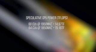
To hit the bottom end 11TF (6x PS4's 1.84TF), a 60 CU graphics core will need to run around 1500MHz, while a fully enabled 64 CU GPU could run around 100MHz slower. To hit the max 15TF, 60 CUs would require around 1950MHz while 64 would need circa 1850MHz. Suffice to say that if the GCN has a structural limitation at 64 Cus, the higher end looks extremely unlikely to pull off. However, based on the kind of speeds extracted from the GPU core in Xbox One X, 1500MHz or a touch higher on a new process doesn't look unfeasible.

If AMD is able to exceed 64 compute units with its new Navi architecture (scalability is mentioned in an early slide), looking at how the silicon area of the Xbox One X's Scorpio Engine could scale on a 7nmFF process, 80 compute units looks viable, with 72 or 76 active. 1500MHz on such a core would propel you towards the top-end of the 11-15TF window. Something to remember is that the faster a chip runs, the hotter it gets, adding extra expense in terms of the cooling solution.

The bottom line, though: a PlayStation 5 due this year simply isn't viable if we're looking for any kind of generational leap. And clearly, the current generation still has much to offer - and practically, it's the time period where both Sony and Microsoft will make some serious money. Drawing the end to this console generation right now simply doesn't make sense - for one, there are no first party games aimed specifically at new hardware that could be released this year.

Q4 2019 is our first viable target for a proper generational leap in console power, but the price of that leap in technology looks daunting. Even in the here and now, the price bubbles in the PC component market are making the high cost of Xbox One X look a lot more attractive. But a relatively large 7nm processor with an Xbox One X-level cooling solution paired with a big upgrade in RAM and some kind of solid-state storage solution? That's a whole new level of expense - and financial viability more than any other factor may well push the arrival of a next-gen PlayStation or Xbox back to 2020.

Avatar image for Grey_Eyed_Elf
Grey_Eyed_Elf

7970

Forum Posts

0

Wiki Points

0

Followers

Reviews: 0

User Lists: 0

#62 Grey_Eyed_Elf
Member since 2011 • 7970 Posts

@ronvalencia: Its NOW competing... The first batch of Zen cores no so much. Its what I said they were behind in core clocks which is the whole point of Ryzen 2 to close that gap but even so a overclocked 8700/8600 would make another gap especially at 1080/1440 100/144Hz gaming.

Avatar image for Grey_Eyed_Elf
Grey_Eyed_Elf

7970

Forum Posts

0

Wiki Points

0

Followers

Reviews: 0

User Lists: 0

#63 Grey_Eyed_Elf
Member since 2011 • 7970 Posts

@GioVela2010: You forgot the most important and critical part of the speculation:

But whether there's a set top-end imposed by the structural limitations of the GCN architecture, or thphysical size of the silicone , it's going to be the frequency of the GPU - based heavily on the capabilities of the 7nm process - that's going to be key in getting that teraflop count as high as possible. Typically, frequencies increase from one process to the next, but the speeds attainable at 7nm are unknown right now. Xbox One X's GPU hits 1172MHz at 16nm, but we're going to need a big bump from the next process - around 30 per cent at the minimum.

To hit the bottom end 11TF (6x PS4's 1.84TF), a 60 CU graphics core will need to run around 1500MHz, while a fully enabled 64 CU GPU could run around 100MHz slower. To hit the max 15TF, 60 CUs would require around 1950MHz while 64 would need circa 1850MHz. Suffice to say that if the GCN has a structural limitation at 64 Cus, the higher end looks extremely unlikely to pull off. However, based on the kind of speeds extracted from the GPU core in Xbox One X, 1500MHz or a touch higher on a new process doesn't look unfeasible.

If AMD is able to exceed 64 compute units with its new Navi architecture (scalability is mentioned in an early slide), looking at how the silicon area of the Xbox One X's Scorpio Engine could scale on a 7nmFF process, 80 compute units looks viable, with 72 or 76 active. 1500MHz on such a core would propel you towards the top-end of the 11-15TF window. Something to remember is that the faster a chip runs, the hotter it gets, adding extra expense in terms of the cooling solution.

Avatar image for GioVela2010
GioVela2010

5566

Forum Posts

0

Wiki Points

0

Followers

Reviews: 0

User Lists: 0

#64  Edited By GioVela2010
Member since 2008 • 5566 Posts

@Grey_Eyed_Elf said:

@GioVela2010: You forgot the most important and critical part of the speculation:

But whether there's a set top-end imposed by the structural limitations of the GCN architecture, or thphysical size of the silicone , it's going to be the frequency of the GPU - based heavily on the capabilities of the 7nm process - that's going to be key in getting that teraflop count as high as possible. Typically, frequencies increase from one process to the next, but the speeds attainable at 7nm are unknown right now. Xbox One X's GPU hits 1172MHz at 16nm, but we're going to need a big bump from the next process - around 30 per cent at the minimum.

To hit the bottom end 11TF (6x PS4's 1.84TF), a 60 CU graphics core will need to run around 1500MHz, while a fully enabled 64 CU GPU could run around 100MHz slower. To hit the max 15TF, 60 CUs would require around 1950MHz while 64 would need circa 1850MHz. Suffice to say that if the GCN has a structural limitation at 64 Cus, the higher end looks extremely unlikely to pull off. However, based on the kind of speeds extracted from the GPU core in Xbox One X, 1500MHz or a touch higher on a new process doesn't look unfeasible.

If AMD is able to exceed 64 compute units with its new Navi architecture (scalability is mentioned in an early slide), looking at how the silicon area of the Xbox One X's Scorpio Engine could scale on a 7nmFF process, 80 compute units looks viable, with 72 or 76 active. 1500MHz on such a core would propel you towards the top-end of the 11-15TF window. Something to remember is that the faster a chip runs, the hotter it gets, adding extra expense in terms of the cooling solution.

in what way did I forget that? I mean I posted it after all.

12.5+ TF in 2020 is pretty much guaranteed

Avatar image for Grey_Eyed_Elf
Grey_Eyed_Elf

7970

Forum Posts

0

Wiki Points

0

Followers

Reviews: 0

User Lists: 0

#65 Grey_Eyed_Elf
Member since 2011 • 7970 Posts

@GioVela2010 said:
@Grey_Eyed_Elf said:

@GioVela2010: You forgot the most important and critical part of the speculation:

But whether there's a set top-end imposed by the structural limitations of the GCN architecture, or thphysical size of the silicone , it's going to be the frequency of the GPU - based heavily on the capabilities of the 7nm process - that's going to be key in getting that teraflop count as high as possible. Typically, frequencies increase from one process to the next, but the speeds attainable at 7nm are unknown right now. Xbox One X's GPU hits 1172MHz at 16nm, but we're going to need a big bump from the next process - around 30 per cent at the minimum.

To hit the bottom end 11TF (6x PS4's 1.84TF), a 60 CU graphics core will need to run around 1500MHz, while a fully enabled 64 CU GPU could run around 100MHz slower. To hit the max 15TF, 60 CUs would require around 1950MHz while 64 would need circa 1850MHz. Suffice to say that if the GCN has a structural limitation at 64 Cus, the higher end looks extremely unlikely to pull off. However, based on the kind of speeds extracted from the GPU core in Xbox One X, 1500MHz or a touch higher on a new process doesn't look unfeasible.

If AMD is able to exceed 64 compute units with its new Navi architecture (scalability is mentioned in an early slide), looking at how the silicon area of the Xbox One X's Scorpio Engine could scale on a 7nmFF process, 80 compute units looks viable, with 72 or 76 active. 1500MHz on such a core would propel you towards the top-end of the 11-15TF window. Something to remember is that the faster a chip runs, the hotter it gets, adding extra expense in terms of the cooling solution.

in what way did I forget that? I mean I posted it after all.

12.5+ TF in 2020 is pretty much guaranteed

How?... Explain to us, we are all interested and waiting.

Ron stay away, let him at least try.

Avatar image for GioVela2010
GioVela2010

5566

Forum Posts

0

Wiki Points

0

Followers

Reviews: 0

User Lists: 0

#66 GioVela2010
Member since 2008 • 5566 Posts

@Grey_Eyed_Elf said:
@GioVela2010 said:
@Grey_Eyed_Elf said:

@GioVela2010: You forgot the most important and critical part of the speculation:

But whether there's a set top-end imposed by the structural limitations of the GCN architecture, or thphysical size of the silicone , it's going to be the frequency of the GPU - based heavily on the capabilities of the 7nm process - that's going to be key in getting that teraflop count as high as possible. Typically, frequencies increase from one process to the next, but the speeds attainable at 7nm are unknown right now. Xbox One X's GPU hits 1172MHz at 16nm, but we're going to need a big bump from the next process - around 30 per cent at the minimum.

To hit the bottom end 11TF (6x PS4's 1.84TF), a 60 CU graphics core will need to run around 1500MHz, while a fully enabled 64 CU GPU could run around 100MHz slower. To hit the max 15TF, 60 CUs would require around 1950MHz while 64 would need circa 1850MHz. Suffice to say that if the GCN has a structural limitation at 64 Cus, the higher end looks extremely unlikely to pull off. However, based on the kind of speeds extracted from the GPU core in Xbox One X, 1500MHz or a touch higher on a new process doesn't look unfeasible.

If AMD is able to exceed 64 compute units with its new Navi architecture (scalability is mentioned in an early slide), looking at how the silicon area of the Xbox One X's Scorpio Engine could scale on a 7nmFF process, 80 compute units looks viable, with 72 or 76 active. 1500MHz on such a core would propel you towards the top-end of the 11-15TF window. Something to remember is that the faster a chip runs, the hotter it gets, adding extra expense in terms of the cooling solution.

in what way did I forget that? I mean I posted it after all.

12.5+ TF in 2020 is pretty much guaranteed

How?... Explain to us, we are all interested and waiting.

Ron stay away, let him at least try.

First of all the 64 CU limit is not guaranteed to be the case with Navi. The “scalability” that has been referenced could very well mean the 64 CU Limit won’t apply.

2nd of all, even with a 64 CU Limit, And 4 being disabled all you need would be a 35-40% clock increase over X1X to achieve 12.5 TF

Xbox 360 Core Clock = 500

pS4 Core Clock = 800

X1 Core Clock = 915

X1X Core Clock = 1172

next gen consoles with 60 CU’s and 1600-1650 clock speeds is not impossible, and DF agrees clearly.

Avatar image for mariokart64fan
mariokart64fan

20828

Forum Posts

0

Wiki Points

0

Followers

Reviews: 101

User Lists: 1

#67 mariokart64fan
Member since 2003 • 20828 Posts

@GioVela2010 so 2019 for Xbox two? I really don't think so

And ps 4 is selling well I don't see any reason why Sony can't just keep support it til 2020 at least:

Avatar image for Grey_Eyed_Elf
Grey_Eyed_Elf

7970

Forum Posts

0

Wiki Points

0

Followers

Reviews: 0

User Lists: 0

#68 Grey_Eyed_Elf
Member since 2011 • 7970 Posts

@GioVela2010 said:
@Grey_Eyed_Elf said:
@GioVela2010 said:
@Grey_Eyed_Elf said:

@GioVela2010: You forgot the most important and critical part of the speculation:

But whether there's a set top-end imposed by the structural limitations of the GCN architecture, or thphysical size of the silicone , it's going to be the frequency of the GPU - based heavily on the capabilities of the 7nm process - that's going to be key in getting that teraflop count as high as possible. Typically, frequencies increase from one process to the next, but the speeds attainable at 7nm are unknown right now. Xbox One X's GPU hits 1172MHz at 16nm, but we're going to need a big bump from the next process - around 30 per cent at the minimum.

To hit the bottom end 11TF (6x PS4's 1.84TF), a 60 CU graphics core will need to run around 1500MHz, while a fully enabled 64 CU GPU could run around 100MHz slower. To hit the max 15TF, 60 CUs would require around 1950MHz while 64 would need circa 1850MHz. Suffice to say that if the GCN has a structural limitation at 64 Cus, the higher end looks extremely unlikely to pull off. However, based on the kind of speeds extracted from the GPU core in Xbox One X, 1500MHz or a touch higher on a new process doesn't look unfeasible.

If AMD is able to exceed 64 compute units with its new Navi architecture (scalability is mentioned in an early slide), looking at how the silicon area of the Xbox One X's Scorpio Engine could scale on a 7nmFF process, 80 compute units looks viable, with 72 or 76 active. 1500MHz on such a core would propel you towards the top-end of the 11-15TF window. Something to remember is that the faster a chip runs, the hotter it gets, adding extra expense in terms of the cooling solution.

in what way did I forget that? I mean I posted it after all.

12.5+ TF in 2020 is pretty much guaranteed

How?... Explain to us, we are all interested and waiting.

Ron stay away, let him at least try.

First of all the 64 CU limit is not guaranteed to be the case with Navi. The “scalability” that has been referenced could very well mean the 64 CU Limit won’t apply.

2nd of all, even with a 64 CU Limit, And 4 being disabled all you need would be a 35-40% clock increase over X1X to achieve 12.5 TF

Xbox 360 Core Clock = 500

pS4 Core Clock = 800

X1 Core Clock = 915

X1X Core Clock = 1172

next gen consoles with 60 CU’s and 1600-1650 clock speeds is not impossible, and DF agrees clearly.

Which is speculation there is no guarantee because as they state they do not know like all of us the impact a 7nm process would actually make.

60cu with 1500Mhz gets you 11tflops... But at what TDP and heat levels?... They don't know its why they don't mention it, they are purely basing their speculation based on the rumoured TFLOP count of a DEVKIT.

Its why its called speculation.

Yet again you seem very very sure to the point where it is guaranteed?...

As for the 64CU limit not being the case with Navi?... Er it is the limit with Navi because Navi is GCN based, the only difference is they can have more than one GPU on a die using infinity fabric, something that probably wont be done for the PS5 again due to TDP and heat.

Avatar image for GioVela2010
GioVela2010

5566

Forum Posts

0

Wiki Points

0

Followers

Reviews: 0

User Lists: 0

#69 GioVela2010
Member since 2008 • 5566 Posts

@Grey_Eyed_Elf said:
@GioVela2010 said:
@Grey_Eyed_Elf said:
@GioVela2010 said:
@Grey_Eyed_Elf said:

@GioVela2010: You forgot the most important and critical part of the speculation:

But whether there's a set top-end imposed by the structural limitations of the GCN architecture, or thphysical size of the silicone , it's going to be the frequency of the GPU - based heavily on the capabilities of the 7nm process - that's going to be key in getting that teraflop count as high as possible. Typically, frequencies increase from one process to the next, but the speeds attainable at 7nm are unknown right now. Xbox One X's GPU hits 1172MHz at 16nm, but we're going to need a big bump from the next process - around 30 per cent at the minimum.

To hit the bottom end 11TF (6x PS4's 1.84TF), a 60 CU graphics core will need to run around 1500MHz, while a fully enabled 64 CU GPU could run around 100MHz slower. To hit the max 15TF, 60 CUs would require around 1950MHz while 64 would need circa 1850MHz. Suffice to say that if the GCN has a structural limitation at 64 Cus, the higher end looks extremely unlikely to pull off. However, based on the kind of speeds extracted from the GPU core in Xbox One X, 1500MHz or a touch higher on a new process doesn't look unfeasible.

If AMD is able to exceed 64 compute units with its new Navi architecture (scalability is mentioned in an early slide), looking at how the silicon area of the Xbox One X's Scorpio Engine could scale on a 7nmFF process, 80 compute units looks viable, with 72 or 76 active. 1500MHz on such a core would propel you towards the top-end of the 11-15TF window. Something to remember is that the faster a chip runs, the hotter it gets, adding extra expense in terms of the cooling solution.

in what way did I forget that? I mean I posted it after all.

12.5+ TF in 2020 is pretty much guaranteed

How?... Explain to us, we are all interested and waiting.

Ron stay away, let him at least try.

First of all the 64 CU limit is not guaranteed to be the case with Navi. The “scalability” that has been referenced could very well mean the 64 CU Limit won’t apply.

2nd of all, even with a 64 CU Limit, And 4 being disabled all you need would be a 35-40% clock increase over X1X to achieve 12.5 TF

Xbox 360 Core Clock = 500

pS4 Core Clock = 800

X1 Core Clock = 915

X1X Core Clock = 1172

next gen consoles with 60 CU’s and 1600-1650 clock speeds is not impossible, and DF agrees clearly.

Which is speculation there is no guarantee because as they state they do not know like all of us the impact a 7nm process would actually make.

60cu with 1500Mhz gets you 11tflops... But at what TDP and heat levels?... They don't know its why they don't mention it, they are purely basing their speculation based on the rumoured TFLOP count of a DEVKIT.

Its why its called speculation.

Yet again you seem very very sure to the point where it is guaranteed?...

As for the 64CU limit not being the case with Navi?... Er it is the limit with Navi because Navi is GCN based, the only difference is they can have more than one GPU on a die using infinity fabric, something that probably wont be done for the PS5 again due to TDP and heat.

I’m not 100% convinced Navi will be limited to 64 CU’s. And clearly neither is Digital Foundry

Avatar image for GioVela2010
GioVela2010

5566

Forum Posts

0

Wiki Points

0

Followers

Reviews: 0

User Lists: 0

#70 GioVela2010
Member since 2008 • 5566 Posts

As for the heat and power consumption.

If someone in mid 2015 told you that in 2017 A new console would be coming out with similar Teraflops to a R9 390X, a 1 month old GPU with a TDP of 285 watts And an MSRP of $430+. You clearly would have balked at the notion because of heat, power consumption, and price. Yet here we are..

Avatar image for GioVela2010
GioVela2010

5566

Forum Posts

0

Wiki Points

0

Followers

Reviews: 0

User Lists: 0

#71 GioVela2010
Member since 2008 • 5566 Posts

@mariokart64fan said:

@GioVela2010 so 2019 for Xbox two? I really don't think so

And ps 4 is selling well I don't see any reason why Sony can't just keep support it til 2020 at least:

I’m not predicting 2019, and neither is Digital Foundry. They say 2020 is most likely, but 2019 is the earliest possibility. Those are not the same thing

Avatar image for Macutchi
Macutchi

10436

Forum Posts

0

Wiki Points

0

Followers

Reviews: 4

User Lists: 0

#72 Macutchi
Member since 2007 • 10436 Posts

took one reply to make me realise i'm well out of my depth in this thread

@Grey_Eyed_Elf said:

They over predict, they always forget TDP... Their TFLOP predictions are skewed by their core clock estimates for which should be taken with a grain of salt considering the TDP of a Vega 64 card is that of two PS4's combined. A 7nm production would obviously help improve TDP with GCN but it will more or less be lower than 12.

Avatar image for 04dcarraher
04dcarraher

23829

Forum Posts

0

Wiki Points

0

Followers

Reviews: 2

User Lists: 0

#73  Edited By 04dcarraher
Member since 2004 • 23829 Posts

@GioVela2010 said:

As for the heat and power consumption.

If someone in mid 2015 told you that in 2017 A new console would be coming out with similar Teraflops to a R9 390X, a 1 month old GPU with a TDP of 285 watts And an MSRP of $430+. You clearly would have balked at the notion because of heat, power consumption, and price. Yet here we are..

not if they know about nm nodes..... again 7nm will not allow a GCN based gpu with 12+ TFLOP and stay within the current power and cooling limits.

Unless AMD moves away from GCN and or vastly improves the performance per watt ratio of their gpus , or console manufactures finally decide to take a hit on profit for better hardware design limits. As it stands Navi in console/s in 2019/2020 will be under 12 TFLOPS..... unless one of those two things happens. Hell even AMD stated Navi in 2019 will be aroound GTX 1080 range which is 10-11 TFLOP for AMD GCN.

Avatar image for osan0
osan0

17817

Forum Posts

0

Wiki Points

0

Followers

Reviews: 1

User Lists: 0

#74 osan0
Member since 2004 • 17817 Posts

an interesting video. i think the key thing with next gen hardware is going to be the customisation.....teh hidden power so to speak. this is just my speculation of course.

on paper i dont think the PS5/X2 will be as impressive as many will hope for. i mean if 64 compute units is it for GCN then its it.

i think DF are getting a bit carried away on the CPU side. given the choice between more CPU cores and more GPU shaders they will go for the latter so i suspect next gen consoles are going to have 1 ryzen CCX available to games: 4 cores and 8 threads with a higher clock. they may also have a couple of jaguar cores for system/OS stuff. devs dont really want more cores. they want each core to be faster instead.

on the GPU side i think 12TF will be the upper limit. a navi 64. if 64 CUs is the limit then its the limit. an impressive jump from a PS4 or X1 but not so much from a pro or X1X.

on paper a pretty solid box. but its the customisation DF allude to that will be key.

instead of looking to have 8 cores/16 threads on the CPU they will be looking to reduce the CPU burden. what can they do at the hardware level to get more work done using less of the CPUs capacity. customised parts of the chip designed to run common game instructions very very quickly.

same on the GPU: how do they get more done with what they have? better customised texture compression to reduce the demand on memory bandwidth. customised instructions that can get more of the GPU working more efficently under certain scenarios. advanced rendering tricks that use customised silicon used at the last stage of the rendering process to give things like post process AA for free.

a sort of mixture of old school console design and using more off the shelf parts. i think this is where the differentiator will be next gen.

Avatar image for FireEmblem_Man
FireEmblem_Man

20248

Forum Posts

0

Wiki Points

0

Followers

Reviews: 7

User Lists: 0

#75 FireEmblem_Man
Member since 2004 • 20248 Posts

DF never considered price, TDP, or macro-economics at all when predicting consoles power. If anything, next-gen systems will be around up to the price of $400 max. We know that both MS and Sony will stick w/AMD both CPU and GPU, so Zen makes sense, but what type of Zen are they using? Will they be using the 1st gen Zen architect for lower cost as Zen 2 will be a bit more pricier? Will the CPU be a custom desktop APU or a custom mobile variant? This is a huge challenge for MS and Sony's R&D team.

Avatar image for biack_goku
BIack_Goku

724

Forum Posts

0

Wiki Points

0

Followers

Reviews: 0

User Lists: 0

#76 BIack_Goku
Member since 2016 • 724 Posts

Apparently Cerny is going around asking developers what they're looking for in the PS5. 2020 release seems almost like a certainty at this point.

Avatar image for GioVela2010
GioVela2010

5566

Forum Posts

0

Wiki Points

0

Followers

Reviews: 0

User Lists: 0

#77 GioVela2010
Member since 2008 • 5566 Posts

@04dcarraher said:
@GioVela2010 said:

As for the heat and power consumption.

If someone in mid 2015 told you that in 2017 A new console would be coming out with similar Teraflops to a R9 390X, a 1 month old GPU with a TDP of 285 watts And an MSRP of $430+. You clearly would have balked at the notion because of heat, power consumption, and price. Yet here we are..

again 7nm will not allow a GCN based gpu with 12+ TFLOP and stay within the current power and cooling limits.

Based on what?

GCN 3.0 on 28nm Fab launched with R9 285 in 2014, 3.3 Teraflops, 190w TDP (359nm Die Size)

GCN 4.0 on 14nm Fab with a RX580 is 6.2 Teraflops with 185w TDP (232mm die zie)

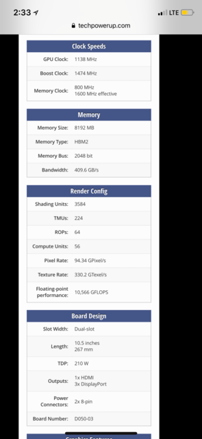
GCN 5.0 on 14nm (Vega 56) 10.55 TF with 210w TDP (486nm die size)

So what on earth would make you believe Navi with GCN 6.0 using 7nm Fab cannot achieve 12 TF at under 200w? I would argue that's a pretty low bar being that its BOTH 7nm Fab AND GCN 6.0

Last time AMD went from one GCN to the next, and ALSO halved the FAB they nearly coubled the TFLOPS, and lowered the TDP.

Avatar image for robert_sparkes
robert_sparkes

7233

Forum Posts

0

Wiki Points

0

Followers

Reviews: 0

User Lists: 5

#78 robert_sparkes
Member since 2018 • 7233 Posts

I find it very strange there's speculation that ms are not doing generations.

Avatar image for lifelessablaze
lifelessablaze

1066

Forum Posts

0

Wiki Points

0

Followers

Reviews: 1

User Lists: 5

#79 lifelessablaze
Member since 2017 • 1066 Posts

I think it's kind of sad that people care about this. If the only bump from new consoles is resolution and framerate then there isn't much to be excited about. There hasn't been any substantial evolution in AI and the fact that nobody cares sends the wrong message to developers.

Avatar image for rhoadsxiommi
rhoadsxiommi

75

Forum Posts

0

Wiki Points

0

Followers

Reviews: 0

User Lists: 5

#80  Edited By rhoadsxiommi
Member since 2018 • 75 Posts

Am i the only guy who misses the 8bit vs 16bit guage for improvement? Seemed much more direct.

Kidding only, of course, i realize the bit wars were a foundation for marketing.

I’m extremely excited to see what the next gen consoles are like. Seriously, though, my favorite videogames right now are shovel knight and the mega man legacy collections.

Games with the highest priority on my “to get” list are totally owlboy and the mega man x legacy collections on the days they are released.

I’m beginning to think nintendo’s “less as more” hardware situation is not so horrible (and i originally had my doubts. My mantra for art has been “more is more,” for a long time)

Avatar image for 04dcarraher
04dcarraher

23829

Forum Posts

0

Wiki Points

0

Followers

Reviews: 2

User Lists: 0

#81  Edited By 04dcarraher
Member since 2004 • 23829 Posts

@GioVela2010 said:
@04dcarraher said:
@GioVela2010 said:

As for the heat and power consumption.

If someone in mid 2015 told you that in 2017 A new console would be coming out with similar Teraflops to a R9 390X, a 1 month old GPU with a TDP of 285 watts And an MSRP of $430+. You clearly would have balked at the notion because of heat, power consumption, and price. Yet here we are..

again 7nm will not allow a GCN based gpu with 12+ TFLOP and stay within the current power and cooling limits.

Based on what?

GCN 3.0 on 28nm Fab launched with R9 285 in 2014, 3.3 Teraflops, 190w TDP (359nm Die Size)

GCN 4.0 on 14nm Fab with a RX580 is 6.2 Teraflops with 185w TDP (232mm die zie)

GCN 5.0 on 14nm (Vega 56) 10.55 TF with 210w TDP (486nm die size)

So what on earth would make you believe Navi with GCN 6.0 using 7nm Fab cannot achieve 12 TF at under 200w? I would argue that's a pretty low bar being that its BOTH 7nm Fab AND GCN 6.0

Last time AMD went from one GCN to the next, and ALSO halved the FAB they nearly coubled the TFLOPS, and lowered the TDP.

lol

best of GCN 3.0 was FuryX and its TDP was near 300w and it provided 8.6 TFLOPS at 28nm

GCN 4.0 best was RX 580. 6.1 TFLOP 14nm with a TDP around 190-200w

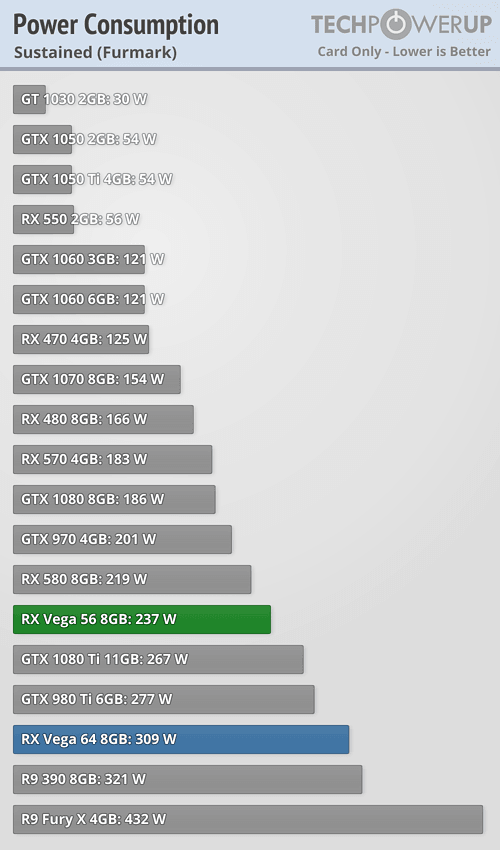
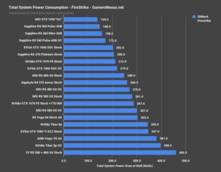
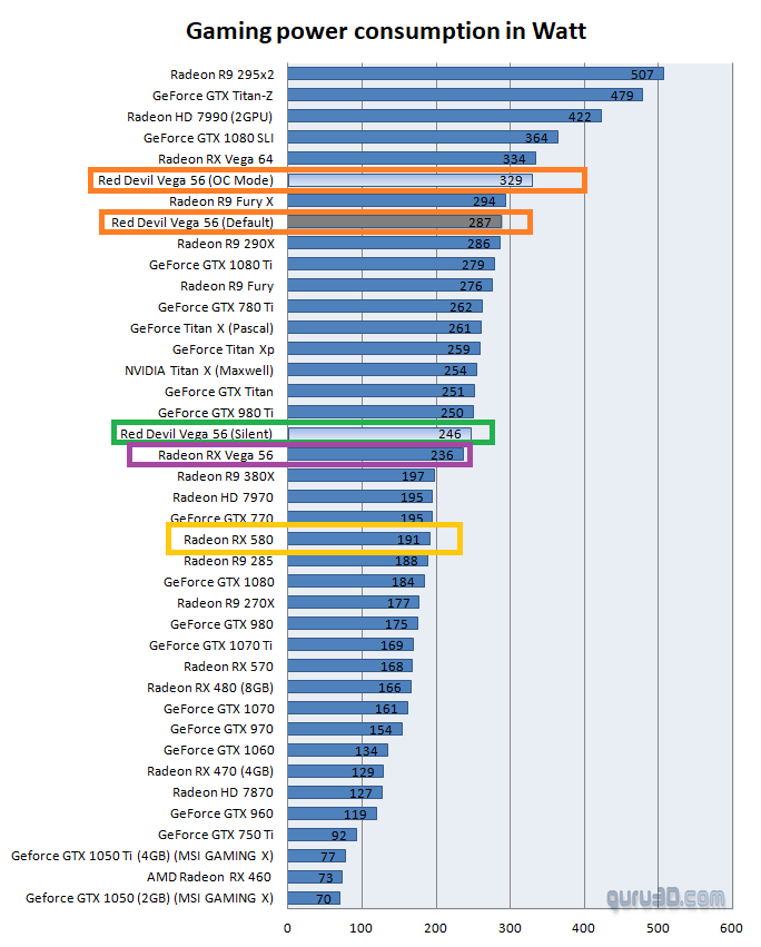
GCN 5.0 Vega 56 does not have a TDP of 210w..... its true usage with reference cooler hovers 235-240w.... Non reference cooler based 56's reach of upto 285w and provide near VEGA 64 performance while 64 TDP is over 330w. All at 14nm.

Vega 64 is 12.5 TFLOP gpu uses over 330w at 14nm even if you can cut power consumption in half by going 7nm which you cant. Your still above the 150w TDP mark just for the gpu.....

Even from 28nm to 14nm going from Fury X to VEGA 64 provided 40% TFLOP increase in performance and going to 14nm from 28nm did not provide 50% less power draw....

Avatar image for GioVela2010
GioVela2010

5566

Forum Posts

0

Wiki Points

0

Followers

Reviews: 0

User Lists: 0

#82  Edited By GioVela2010
Member since 2008 • 5566 Posts

You’re an idiot, Vega 56 uses 7% more power than a RX 580...

X1X is putting out RX 580 levels of power and tests have shown 185w during 4K Gaming “150 watt limit”

lol

Avatar image for airraidjet
airraidjet

834

Forum Posts

0

Wiki Points

0

Followers

Reviews: 2

User Lists: 0

#83 airraidjet
Member since 2006 • 834 Posts

@lifelessablaze said:

I think it's kind of sad that people care about this. If the only bump from new consoles is resolution and framerate then there isn't much to be excited about. There hasn't been any substantial evolution in AI and the fact that nobody cares sends the wrong message to developers.

The biggest leap next gen consoles will make will be from the CPU, allowing greater world simulation, physics, A.I. and things not related to graphics. After that, the next biggest bump will be to the complexity of the graphics and lighting. Going from the lowest common denominator (XBone's 1.3 TF) to a new base of 10-12 TF, games will get a significant if not massive boost to overall graphic sophistication. The last and smallest improvement will be to pixel resolution (we're already getting a lot of native 4K stuff on Xbox One X). Going from 1080p to 4K is pretty big, but not as big as the improvements to games in other areas I just mentioned.

The issue of framerate will always be a choice developers make. While the new Zen CPU architecture will allow for potentially better framerates than current-gen, it's not 100% given. Many devs will always choose ~30fps over 60fps, but at least with PS5 and Xbox Next, the CPU won't be crippling as it is this gen with all the consoles based on Jaguar.

Avatar image for 04dcarraher
04dcarraher

23829

Forum Posts

0

Wiki Points

0

Followers

Reviews: 2

User Lists: 0

#84  Edited By 04dcarraher
Member since 2004 • 23829 Posts

@GioVela2010 said:

You’re an idiot, Vega 56 uses 7% more power than a RX 580...

X1X is putting out RX 580 levels of power and tests have shown 185w during 4K Gaming “150 watt limit”

lol

lol try again.... its more like 20% reference vs reference....... vega 56 will use more power when cooling is sufficient boosting clocks..... Vega 56 using 236w using reference cooler..... X1X is using 35-40w less than RX 580 is because it dont have as much to power ie its dedicated memory etc....

What is funny is that GTX 1080 using less power than a 14nm RX 580 at 16nm and perform on par with a 14nm Vega 56 while using 25% less power.

For Navi to reach 12 TFLOP at 7nm you can expect it to use more than 150w....

Avatar image for GioVela2010
GioVela2010

5566

Forum Posts

0

Wiki Points

0

Followers

Reviews: 0

User Lists: 0

#85 GioVela2010
Member since 2008 • 5566 Posts

@04dcarraher said:
@GioVela2010 said:

You’re an idiot, Vega 56 uses 7% more power than a RX 580...

X1X is putting out RX 580 levels of power and tests have shown 185w during 4K Gaming “150 watt limit”

lol

lol try again.... its more like 20% reference vs reference....... vega 56 will use more power when cooling is sufficient boosting clocks..... Vega 56 using 236w using reference cooler..... X1X is using 35-40w less than RX 580 is because it dont have as much to power ie its dedicated memory etc....

What is funny is that GTX 1080 using less power than a 14nm RX 580 at 16nm and perform on par with a 14nm Vega 56 while using 25% less power.

For Navi to reach 12 TFLOP at 7nm you can expect it to use more than 150w....

Lmao this is fucking stupid. Why would you use versions of cards that are more inefficient in power per watt than the stock gpu at stock speeds? You’re a joke

Boost Mode is not the same as being overclocked, manufacture TDP specs account for Boost Mode.

Console GPU’s will be set to max efficiency, They won’t keep cranking up power consumption 40% to get a 5% performance boost.

Avatar image for 04dcarraher
04dcarraher

23829

Forum Posts

0

Wiki Points

0

Followers

Reviews: 2

User Lists: 0

#86  Edited By 04dcarraher
Member since 2004 • 23829 Posts

aww too bad your ignoring that vega 56 is using more than the suggested 210w on that chart ...... let alone other reviews showing 230w+ typical gaming loads..... A stock vega 56 uses anywhere between 230-240w with full loads.... not the 210w.

Once you come to terms that stock/reference RX 580 and vega 56 use more power than the spec sheet AMD provided you will sleep better....

Avatar image for GioVela2010
GioVela2010

5566

Forum Posts

0

Wiki Points

0

Followers

Reviews: 0

User Lists: 0

#87  Edited By GioVela2010
Member since 2008 • 5566 Posts

@04dcarraher said:

aww too bad your ignoring that vega 56 is using more than the suggested 210w on that chart ...... let alone other reviews showing 230w+ typical gaming loads..... A stock vega 56 uses anywhere between 230-240w with full loads.... not the 210w.

Once you come to terms that stock/reference RX 580 and vega 56 use more power than the spec sheet AMD provided you will sleep better....

Except your proving Vega 56 only uses 6-7% more power than a RX580 lmao.

And X1X has better than 580 performance...

So how does all this prove Navi on 7nm fab cannot reach 12.5 TF again?

Avatar image for superbuuman
superbuuman

6400

Forum Posts

0

Wiki Points

0

Followers

Reviews: 14

User Lists: 0

#88  Edited By superbuuman
Member since 2010 • 6400 Posts

will be using ryzen if they stick with AMD ..but I don't think it will be using be the latest Ryzen released in 2019. :P

Avatar image for 04dcarraher
04dcarraher

23829

Forum Posts

0

Wiki Points

0

Followers

Reviews: 2

User Lists: 0

#89  Edited By 04dcarraher
Member since 2004 • 23829 Posts

That is because of furmark..... gaming usage sits around 15-20% difference.....

Even still the reason why the X1X performs better is because of its cache size and better memory bandwidth..... Fact is that X1X's GPU TDP spec does not include everything the RX 580 has to power as well.... dedicated gpus also have to power its cooling and its own memory etc..... which add to the power usage. Vram can use 20-30w easily..... So that 150w spec of the X1X gpu is not that much better than a RX 580 gpu core once you factor in the extra components.

This is what you seem not to understand..... In a restricted environment power, heat/cooling and size is everything. I never once said Navi couldn't reach 12+ TFLOP I said it cant in a console environment with their current design limits......

For Navi to reach 12+ TFLOP surpass the current TDP limits in consoles even using 7nm. Like I said unless AMD revamps GCN in its performance per watt (unlikely) or console makers eat some profit for bigger design limits. GCN has not improved much in the last 3 revisions when it comes to power usage. GCN's power saving have been from using smaller nm nodes.... Going from 28nm Fury X to 14nm Vega 56 sees around 20% increase in TFLOPS and saved 20% in power.

So again Navi in 7nm and trying to get it to 12+ TFLOP means that the gpu will be beyond the current 150w X1X gpu. So unless Sony decides to increasethe power and cooling restrictions in the design 9-10 TFLOPS will be more likely.

Avatar image for GioVela2010
GioVela2010

5566

Forum Posts

0

Wiki Points

0

Followers

Reviews: 0

User Lists: 0

#90  Edited By GioVela2010
Member since 2008 • 5566 Posts

@04dcarraher said:
@GioVela2010 said:

You’re an idiot, Vega 56 uses 7% more power than a RX 580...

X1X is putting out RX 580 levels of power and tests have shown 185w during 4K Gaming “150 watt limit”

lol

lol try again.... its more like 20% reference vs reference....... vega 56 will use more power when cooling is sufficient boosting clocks..... Vega 56 using 236w using reference cooler..... X1X is using 35-40w less than RX 580 is because it dont have as much to power ie its dedicated memory etc....

What is funny is that GTX 1080 using less power than a 14nm RX 580 at 16nm and perform on par with a 14nm Vega 56 while using 25% less power.

For Navi to reach 12 TFLOP at 7nm you can expect it to use more than 150w....

Your overclocked Vega benchmarks are 100% pointless, efficiency goes down the more you overclock. Heck they can lower the Vega 56 clocks a tad and get even better performance per watt. And i wont even get into undervolting.

But what else should i expect from you, you're the same genius that was predicting HD 7750 for PS4 just 6 months before it launched because of these same TDP limitations. Howd that prediction work out for you? You were only off by 100%

Avatar image for ronvalencia
ronvalencia

29612

Forum Posts

0

Wiki Points

0

Followers

Reviews: 1

User Lists: 0

#91  Edited By ronvalencia
Member since 2008 • 29612 Posts

@04dcarraher said:
@Grey_Eyed_Elf said:
@GioVela2010 said:
@04dcarraher said:

lol expecting 7nm navi to be 12+ TFLOP..... Navi in 2019 is suppose to be around gtx 1080 level of performance in which means under 12 TFLOPS.....

Navi is not one GPU.

Having one Navi GPU at 1080 performance for $250 doesn’t mean a more powerful Navi GPU for consoles in 2020, or even 2019 isn’t possible.

Polaris 460 from August 2016 is 2.1 TF

Polaris 580 from April 2017 is 6.2 TF.

Vega 56 uses about 15% more power than a RX 580. That’s not that much.

X1X is doing what it’s doing, embarrassing the 580 while using less power.

I’ve never seen the Watts surpass 190 while gaming in any benchmarks with X1X as a whole system, while a 580 alone will go over 220 rregularly. Yet the X1X put the smack down on the 580 in Far Cry 5.

Xbox 360 doubled power consumption over its predecessor, next gen consoles using 10-15% more power consumption isn’t out of question.

Where to start...

Polaris 480 came out with the 460... and has a TFLOP count of 5.8 with after market cards hitting 6.1-6.2 due to the core clock overclock.

580 was a refresh of the 480... Same chip just higher core clock due to the better cooling and the additional 6pin power connector which is why it overclocked better and which is why it had the better TFLOP count. A console doesn't have the luxury of increasing the TDP so if its going to use a Navi chip it will be the same performance unless they break the 200w law.

The only way you can increase the TFLOP count without increasing TDP is to lower the clocks and increase the CU units... But Navi is based on GCN which tops out at 64 CU's, so even so regardless of when they release it if it is using Navi it will be the same level of performance regardless of year released because of the TDP limit on consoles.

Wrong again there gio......

Navi as it stands is a single gpu and tops out at 64 CU's like what Grey stated . AMD's interconnect technology with Navi as a test bed (maybe), even if you get two 64+64 CU Navi gpu's stacked its beyond a console's price, power and cooling limits.... Even with 7nm an 64 CU GCN based gpu with same performance as Vega 64 would have more than a 150w TDP. For a Console using Navi you have only a couple options more CU's with much lower clocks or fewer CU's with higher clocks.

VEGA 56 uses more than 15% more power than RX 580... when given proper cooling the 56 will can get itself to the point of using 285w.... Getting near the performance of the VEGA 64..... and using nearly 35% more power than 580.

With similar TDP target, GPU chip size and heat pipe cooling solution, PS4 Pro has 2.3X TFLOPS gain over PS4 and that's shifting from 28 nm to 16 nm process tech.

If the pattern holds true for 16 nm to 7 nm shift, PS4 Pro's 4.2 TFLOPS x 2.3X = 9.66 TFLOPS. 7 nm process tech can give AMD/Sony 2X scale units count e.g.

32 ROPS --> 64 ROPS,

2MB L2 cache ---> 4MB L2 cache

4.2 TFLOPS FP32 ---> 9.66 TFLOPS FP32

Xbox One X has vapor cooler not a heat pipe solution.

If the pattern holds true for 16 nm to 7 nm shift, X1X's 6 TFLOPS x 2.3X = 13.8 TFLOPS. 7 nm process tech can give AMD/MS 2X scale units count e.g.

32 ROPS --> 64 ROPS,

2MB L2 cache ---> 4 MB L2 cache

2MB render cache ---> 4 MB render cache

6 TFLOPS FP32 ---> 13.8 TFLOPS FP32

Vega L2 cache for ROPS and TMUs are unified while it's split on X1X's version

AMD GPUS has a power curve problem i.e. disproportional power consumption increase near clock speed wall. This is why AMD has shifted some of key Ryzen's engineers into RTG

Avatar image for 04dcarraher
04dcarraher

23829

Forum Posts

0

Wiki Points

0

Followers

Reviews: 2

User Lists: 0

#92  Edited By 04dcarraher
Member since 2004 • 23829 Posts
@GioVela2010 said:

Your overclocked Vega benchmarks are 100% pointless, efficiency goes down the more you overclock. Heck they can lower the Vega 56 clocks a tad and get even better performance per watt. And i wont even get into undervolting.

But what else should i expect from you, you're the same genius that was predicting HD 7750 for PS4 just 6 months before it launched because of these same TDP limitations. Howd that prediction work out for you? You were only off by 100%

Fact is the you cant or wont understand the point..... To get to 12 TFLOPS or beyond power usage with GCN goes up its power curve get worse the higher you go with clocks..... Fact is a stock 10.5 TFLOP VEGA 56 uses more than 230w... a 12.5 TFLOP Vega 64 uses over 330w, a overclocked vega 56 that's 11+ TFLOP uses upto 290w. 12+ TFLOP Navi even at 7nm is going to be beyond 150w TDP ....

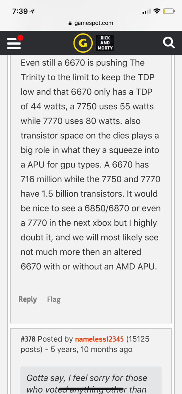
The only time 7750 came into the conversation was when PS4 devkit was rumored that it was based on AMD A10 APU..... I quote "AMD Trinity based APU's are suppose to able to contain igp's that are as fast as an AMD 7750 and that only has a 55w TDP very possible in seeing that type of gpu in the APU. A 7750 is well over 4x stronger then the measly PS3 cell+RSX."

Once the 1.8TFLOP number came out we knew then its gpu was more inline with a modified 7850 than the state of available APU's at the time.

Avatar image for UssjTrunks
UssjTrunks

11299

Forum Posts

0

Wiki Points

0

Followers

Reviews: 0

User Lists: 0

#93  Edited By UssjTrunks
Member since 2005 • 11299 Posts

Why do console peasants always drone on about teraflops? No one in PC gaming talks about it because it's a meaningless buzzword.

At the end of the day, whatever hardware you get is going to be a low end piece of crap (somewhere around xx50/60 Nvidia performance, as usual). There is no way to release a $500 console without using junk hardware.

Avatar image for ronvalencia
ronvalencia

29612

Forum Posts

0

Wiki Points

0

Followers

Reviews: 1

User Lists: 0

#94  Edited By ronvalencia
Member since 2008 • 29612 Posts

@04dcarraher said:
@GioVela2010 said:

Your overclocked Vega benchmarks are 100% pointless, efficiency goes down the more you overclock. Heck they can lower the Vega 56 clocks a tad and get even better performance per watt. And i wont even get into undervolting.

But what else should i expect from you, you're the same genius that was predicting HD 7750 for PS4 just 6 months before it launched because of these same TDP limitations. Howd that prediction work out for you? You were only off by 100%

Fact is the you cant wont understand the point..... To get to 12 TFLOPS or beyond power usage with GCN goes up..... Fact is a stock 10.5 TFLOP VEGA 56 uses more than 230w... a 12.5 TFLOP Vega 64 uses over 330w, a overclocked vega 56 that's 11+ TFLOP uses upto 290w. 12+ TFLOP Navi even at 7nm is going to be beyond 150w TDP ....

PS4 based on the specs I stated 7850 type of performance not 7750......

You're not stating facts from GlobalFoundries 7 nm >60 percent power consumption reduction improvement from 14 nm.

https://www.globalfoundries.com/technology-solutions/cmos/performance/7nm-finfet

This technology provides world-class performance, power, area and cost advantages from 7nm scaling. Based on 3D FinFET transistor architecture and optical lithography with EUV compatibility at key levels, 7LP technology delivers more than twice the logic and SRAM density, and either >40% performance boost or >60% total power reduction, compared to 14nm foundry FinFET offerings.

For Vega 64, 60 percent power reduction from 330 watts lands on 132 watts. This is RX-480 power consumption range. About 2.2X perf/watt improvement.

For Vega 56, 60 percent power reduction from 230 watts lands on 92 watts.

Xbox One X consumes 174 watts with Gears of War 4 in the higher fidelity visual mode.

Xbox One X consumes 174 watts with Gears of War 4 in the higher fidelity visual mode.

PS4 Pro's Infamous First Light 4K consumes 155 watts.

">40% performance boost" deals with clock speed boost.

A single NAVI design could aim for RX-580's power consumption while higher end aims at Vega 54/64's power consumption ie. enough to cover GTX 1080 Ti or Titan V level. Don't expect AMD to target GTX 2080 Ti (beyond Titan XP, Titan V)... Not factoring Ryzen engineering team improving RTG's higher clock speed targets. Any further improvements are up to RTG's micro-architecture improvements.

DX Raytracing compute shaders are less influenced by ROPS unit limitations i.e. it's pure TFLOPS, mostly TMUs (read/write) and tile cache rendering to L2 cache..

Avatar image for 04dcarraher
04dcarraher

23829

Forum Posts

0

Wiki Points

0

Followers

Reviews: 2

User Lists: 0

#95  Edited By 04dcarraher
Member since 2004 • 23829 Posts

Your not going to get 60% power reduction by going to 7nm from 14nm with any GCN keeping the Vega 64 performance numbers.....

You have to read the fine print in what GF stated "either >40% performance boost or >60% total power reduction, compared to 14nm foundry FinFET offerings."

That's why they have the "or" and not "&"...

hell GF also stated "from 14nm area scaling. 14LPP technology can provide up to 55% higher device performance and 60% lower total power compared to 28nm technologies."

Going from 28nm to 14nm, saved AMD 20% surface area while able to pack 30% more transistors with VEGA 64 vs FuryX however power usage savings does not reach the 60% claims.......

GCN performance per watt sucks..... The higher the clocks their power curve gets worse.

Suggesting 132w for vega 64 performance with 7nm isnt even close, expect 7nm gcn with Vega 64 performance to more in line with 190w range. while vega 56 range usage in the 165w range. 9-10 TFLOP GCN for PS5 is totally doable without having to vastly investing more into power and cooling resources.

then we have think about the Zen cpu ether it being a ~3ghz eight core or quad core with SMT clocked higher adds more power and heat into the mix.

So the idea of 12 14 or higher TFLOP based gpu in PS5 in 2019 or 2020 is highly unlikely unless Sony is prepared to take a hit in their profit ratio.

Avatar image for GioVela2010
GioVela2010

5566

Forum Posts

0

Wiki Points

0

Followers

Reviews: 0

User Lists: 0

#96 GioVela2010
Member since 2008 • 5566 Posts

That means the Teraflop stays at 12.6, while power consumption goes down 132w with Vega 64.

Nobody is saying anything about adding 40% from 12.6 to achieve 17.6 TFLOPS .

to achieve 17.6 TFLOpS power consumption would need to stay stagnant

@04dcarraher said:

Your not going to get 60% power reduction by going to 7nm from 14nm with any GCN keeping the Vega 64 performance numbers.....

You have to read the fine print in what GF stated "either >40% performance boost or >60% total power reduction, compared to 14nm foundry FinFET offerings."

Avatar image for GioVela2010
GioVela2010

5566

Forum Posts

0

Wiki Points

0

Followers

Reviews: 0

User Lists: 0

#97 GioVela2010
Member since 2008 • 5566 Posts

@04dcarraher said:
@GioVela2010 said:

Your overclocked Vega benchmarks are 100% pointless, efficiency goes down the more you overclock. Heck they can lower the Vega 56 clocks a tad and get even better performance per watt. And i wont even get into undervolting.

But what else should i expect from you, you're the same genius that was predicting HD 7750 for PS4 just 6 months before it launched because of these same TDP limitations. Howd that prediction work out for you? You were only off by 100%

Fact is the you cant or wont understand the point..... To get to 12 TFLOPS or beyond power usage with GCN goes up its power curve get worse the higher you go with clocks..... Fact is a stock 10.5 TFLOP VEGA 56 uses more than 230w... a 12.5 TFLOP Vega 64 uses over 330w, a overclocked vega 56 that's 11+ TFLOP uses upto 290w. 12+ TFLOP Navi even at 7nm is going to be beyond 150w TDP ....

PS4 based on the performance specs/rumors I stated 7850 type of performance not 7750......

Quotes from back than are broken, but it’s not hard to figure out where your quotes start..

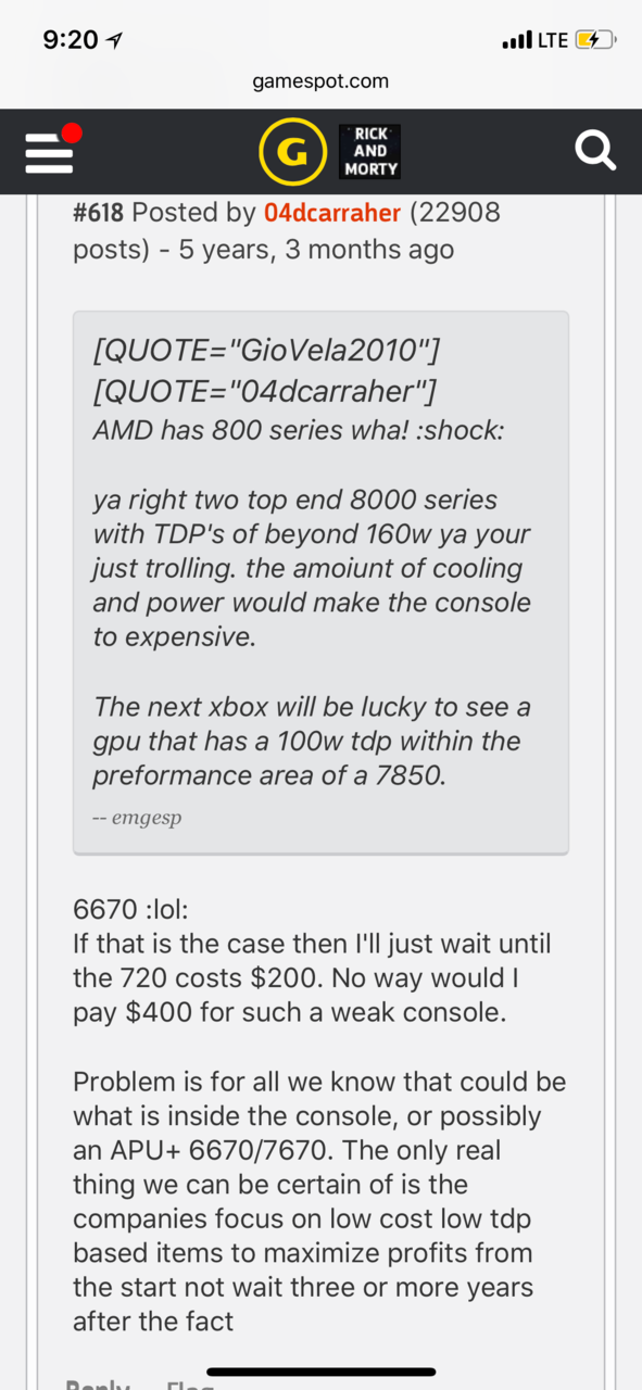
6670 lmao

7860 in PS4 ended up blowing that away. Yes I made up 7860 just now

Shit even when someone almost nailed Xbox One (Bulldozer + 7770) in the last quote, your counter ended up being wrong.

Avatar image for 04dcarraher
04dcarraher

23829

Forum Posts

0

Wiki Points

0

Followers

Reviews: 2

User Lists: 0

#98  Edited By 04dcarraher
Member since 2004 • 23829 Posts

@GioVela2010 said:

That means the Teraflop stays at 12.6, while power consumption goes down 132w with Vega 64.

Nobody is saying anything about adding 40% from 12.6 to achieve 17.6 TFLOPS .

to achieve 17.6 TFLOpS power consumption would need to stay stagnant

Not going happen ,GCN can not achieve the 60% saving while trying to keep performance the same. going 28nm to 14nm did not achieve anything near 60% savings that Global foundries stated from 28nm to 14nm.... for example with FuryX vs Vega 64.... gained around 40% performance but increased power usage 10% so your looking at around 40% power savings.

Expect 190w with Navi aimed at 12 TFLOP and about 165w with Vega 56 10 TFLOP.

Avatar image for 04dcarraher
04dcarraher

23829

Forum Posts

0

Wiki Points

0

Followers

Reviews: 2

User Lists: 0

#99  Edited By 04dcarraher
Member since 2004 • 23829 Posts

@GioVela2010:

back then where there was nothing to base the next consoles on at all..... We were all going by early rumors and what was current ie AMD APU's at that time.... PS4 devkit was also rumored to use an A10 AMD APU ...... So you had to go back to late 2012 and early 2013 posts to show that me suggesting 6670-7750 type of gpus in APU's could be in those consoles..... really?

..... This time with X1X and PS4 pro and PS5 we knew and know alot more with what is in the playing field..... Current rumor with navi to be in PS5, AMD states Navi to be gtx 1080 contender aka vega 56 not 1080ti or Nvidia's new 1170+ or vega 64. Is the not the same unknown factor of what AMD was cooking or MS or Sony's targets for profit back then in 2013.

We have no idea if Sony plans on to throw more money into power and cooling for a 12 or 14 or whatever tflop gpu, But the current trends show less.

Avatar image for GioVela2010
GioVela2010

5566

Forum Posts

0

Wiki Points

0

Followers

Reviews: 0

User Lists: 0

#100 GioVela2010
Member since 2008 • 5566 Posts

@04dcarraher said:
@GioVela2010 said:

That means the Teraflop stays at 12.6, while power consumption goes down 132w with Vega 64.

Nobody is saying anything about adding 40% from 12.6 to achieve 17.6 TFLOPS .

to achieve 17.6 TFLOpS power consumption would need to stay stagnant

Not going happen ,GCN can not achieve the 60% saving while trying to keep performance the same. going 28nm to 14nm did not achieve anything near 60% savings that Global foundries stated from 28nm to 14nm.... for example with FuryX vs Vega 64.... gained around 40% performance but increased power usage 10% so your looking at around 40% power savings.

Expect 190w with Navi aimed at 12 TFLOP and about 165w with Vega 56 10 TFLOP.

Vega isn’t as efficient as it could be because AMD has s chasing Nvidia performance. If they focused on performance per watt Instead of catching up to Nvidia the results would be much better suited for consoles.

just take a look around the web and see the results people are getting wit’s underclocked and undervomter Vegas, 90-95% if the performance while cutting back 40-50% on power consumption.

Sure not everyone will get that dramatic of a gain in performance per watt, but AMD could definitly do better if that was there focus, instead of being scared to be left in the dust by Nvidia in overall power.