RUMORS: Sony PS5 Spec Leaks

  • 110 results
  • 1
  • 2
  • 3
Avatar image for ronvalencia
ronvalencia

29612

Forum Posts

0

Wiki Points

0

Followers

Reviews: 1

User Lists: 0

#101  Edited By ronvalencia
Member since 2008 • 29612 Posts

@Grey_Eyed_Elf said:

@ronvalencia:

...And how did Xbox One X a premium priced mid generation console achieve 6TFLOPS at 150w TDP?... They used a older GCN 2.0 architecture for price and yields and had slower clocks than a RX 480 which can boost to 1250-1300MHz and be 6TFLOPs with a 150w TDP with less 4 Less CU's.

The X1X does nothing special their is no magic behind it at all, its TDP is inline with its CU count and core clocks for GCN. If a RX 580 was clocked to 1.17GHz like a X1X and had its same CU count it will more than likely be at the same 150-175 TDP.

You act like the X1X put a turned a 250w GCN chip into a 150w magic power house, it didn't... Its TDP is a direct result of clocks and CU counts on GCN. You move the CU count up then down goes the clock speeds and vice versa when it comes to hitting the TDP.

NOW:

Rumours/leaks PS5:

  • Navi 10 Lite
  • 1.8GHz clock speeds

Rumours/leaks Navi:

  • Navi 10 48CU 160w
  • Navi 10 52CU 175w
  • Navi 10 56CU 190w

Now... Witch one will be the Navi 10 lite?

If you think AMD will be releasing a 190w 56 CU GPU on PC and then a 56 CU GPU on a console at 150w with clock speeds at 1.8GHz then your even more of a gullible fool than I thought.

Another leak/rumour is that Navi won't hit Vega 20 clocks... A standard Randeon 7 boosts to 1750MHz and can hit 1.9-2GHz with overclocking.

Again the rumours/leaks from Navi are HEAVILY conflicting with the bull-shit fanboy leaks of PS5 spec's when it comes to the GPU.

56 CU at 1.8GHz on GCN at 150w?...

Sh** man based on the TDP of Navi 10 and the 1.8GHz PS5 rumour they would need to take a 48 CU Navi 10 and cut 4 CU's to get 150w, because there is no way that 48CU 160w chip is even hitting 1.8GHz on desktop without dual fans and not going under 70c.

Xbox One X's 44 CU has all the Polaris gfx8 compute updates with extras e.g.

1. Variable shader rate like feature which doesn't exist in Polaris/Hawaii/Tonga/Fury

2. ROPS with 2 MB render cache design which doesn't exist in Polaris/Hawaii/Tonga/Fury

https://gpucuriosity.wordpress.com/2017/09/10/xbox-one-xs-render-backend-2mb-render-cache-size-advantage-over-the-older-gcns/

X1X GPU has Polaris 2MB L2 cache for TMUs with 2 MB render cache for ROPS, hence X1X's GPU is between Polaris and Vega when it comes to cache design. X1X GPU's total L2 + render cache storage is 4MB.

Vega 56/64/VII has unified 4MB L2 cache for both ROPS and TMUs

Hawaii (GCN 2.0) has 1MB L2 cache for TMUs with tiny kilobytes render cache for ROPS.

Polaris 10/20/30 has 2MB L2 cache with tiny kilobytes render cache for ROPS.

@Grey_Eyed_Elf said:

The X1X does nothing special their is no magic behind it at all, its TDP is inline with its CU count and core clocks for GCN.

Bullshit, Polaris doesn't have X1X's 2MB render cache!

Xbox One X dev kit has the full Scorpio GPU has 44 active CU with 6.6 TFLOPS at 1172Mhz (base clock not boost mode) . Retail game console market doesn't allow PC's "XT" and "Pro" SKU difference.

If a game console is built around Polaris 10/20/30 (RX-480/RX-580/RX-590 respectively) design, the console would have 32 active CU with 4 CU disabled for yield issues.
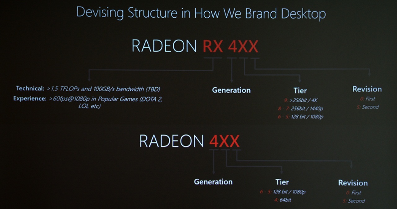
Polaris GPU with greater than 256bit bus was hinted i.e. RX 490. This GPU configuration wasn't released for the PC market, but it was used for Xbox One X.

Try again.

For RTX 2080 Ti (not factoring Tensor and RT cores) vs GTX 1080 Ti, NVIDIA done the following

  • doubled the unified L2 cache in GTX 1080 Ti's 3 MB into 6 MB
  • added rapid pack maths features (from Volta)
  • added discrete integer CUDA units
  • added variable shader rate feature
  • added async compute scheduler with multiple concurrent context support (from Volta)
  • added higher clock speed
  • added more CUDA FP cores
  • improve register storage vs CUDA core count ratio (GCN like, from Volta)
  • improved memory compression
  • 'etc'

RTX 2080 Ti is an upgraded GTX 1080 Ti is an upgraded GTX 980 Ti. 88 ROPS and six GPC units are common designs from GTX 980 Ti to RTX 2080 Ti and it's a good foundation for higher TFLOPS scaling.

The main difference between AMD and NVIDIA is the six geometry-raster engine with 96 ROPS foundation vs four geometry-raster engine with 64 ROPS foundation.

@Grey_Eyed_Elf said:

If you think AMD will be releasing a 190w 56 CU GPU on PC and then a 56 CU GPU on a console at 150w with clock speeds at 1.8GHz then your even more of a gullible fool than I thought.

Don't put words into my mouth. I purposely leaved out the final clock speed for 7nm era game consoles.

Avatar image for Grey_Eyed_Elf
Grey_Eyed_Elf

7970

Forum Posts

0

Wiki Points

0

Followers

Reviews: 0

User Lists: 0

#102 Grey_Eyed_Elf
Member since 2011 • 7970 Posts

@ronvalencia:

Alright Ron, keep running away from the issue.

56 CU, 1.8GHz GCN Chip at 150w is not going to happen. 52 at best but with lower clock speeds than the desktop counter parts.

12.9 TFLOPS. Get out man stop feeding the ignorant here on the forum with false hope of GCN. Its just not happening... As I said for the 3rd time there is a clear conflict with PS5 "rumours" vs the leaks for Navi... They don't align one bit.

Avatar image for ronvalencia
ronvalencia

29612

Forum Posts

0

Wiki Points

0

Followers

Reviews: 1

User Lists: 0

#103  Edited By ronvalencia
Member since 2008 • 29612 Posts

@Grey_Eyed_Elf said:

@ronvalencia:

Alright Ron, keep running away from the issue.

56 CU, 1.8GHz GCN Chip at 150w is not going to happen. 52 at best but with lower clock speeds than the desktop counter parts.

12.9 TFLOPS. Get out man stop feeding the ignorant here on the forum with false hope of GCN. Its just not happening... As I said for the 3rd time there is a clear conflict with PS5 "rumours" vs the leaks for Navi... They don't align one bit.

Don't put words into my mouth. I purposely leaved out the final clock speed for 7nm era game consoles.
Your argument being attached to me is fake news.

Avatar image for ronvalencia
ronvalencia

29612

Forum Posts

0

Wiki Points

0

Followers

Reviews: 1

User Lists: 0

#104  Edited By ronvalencia
Member since 2008 • 29612 Posts

@Grey_Eyed_Elf said:

@ronvalencia:

Alright Ron, keep running away from the issue.

56 CU, 1.8GHz GCN Chip at 150w is not going to happen. 52 at best but with lower clock speeds than the desktop counter parts.

12.9 TFLOPS. Get out man stop feeding the ignorant here on the forum with false hope of GCN. Its just not happening... As I said for the 3rd time there is a clear conflict with PS5 "rumours" vs the leaks for Navi... They don't align one bit.

Loading Video...

Real time power consumption for stock VII vs Vega 64 LC at +1700 Mhz OC+UV. Under volting VII dampens the power spikes to rival RTX 2080's performance per watts.

Stock VII is hovering around 170 to 233 watts. VRMs must handle the short power spikes to avoid program crash.

Avatar image for ronvalencia
ronvalencia

29612

Forum Posts

0

Wiki Points

0

Followers

Reviews: 1

User Lists: 0

#105  Edited By ronvalencia
Member since 2008 • 29612 Posts

@Grey_Eyed_Elf said:

@ronvalencia:

Alright Ron, keep running away from the issue.

56 CU, 1.8GHz GCN Chip at 150w is not going to happen. 52 at best but with lower clock speeds than the desktop counter parts.

12.9 TFLOPS. Get out man stop feeding the ignorant here on the forum with false hope of GCN. Its just not happening... As I said for the 3rd time there is a clear conflict with PS5 "rumours" vs the leaks for Navi... They don't align one bit.

Without 7nm EUV and/or power management improvements to dampen power spike problems with VII, I don't advocate 1800 Mhz for PS5's NAVI 56 CU

7 nm improvements would be built on X1X's GPU with 44 CU at 1172 Mhz.

https://www.tomshardware.com/news/tsmc-7nm-node-process-euv,39097.html

NVIDIA's Volta V100 is based on 12FF nm despite being the same density as 16 nm

Nano-meter bullshit marketing example from TSMC. According to TSMC, 16 nm = 12 nm LOL

TSMC has three 7nm generations

1st gen, 7nm Pro

2nd gen, 7nm+

3rd gen, 6 nm, still compatible with 7nm design rules.

https://www.anandtech.com/show/12677/tsmc-kicks-off-volume-production-of-7nm-chips

The 7 nm node is a big deal for the foundry industry in general and TSMC in particular. When compared to the CLN16FF+ technology (TSMC’s most widely used FinFET process technology) the CLN7FF will enable chip designers to shrink their die sizes by 70% (at the same transistor count), drop power consumption by 60%, or increase frequency by 30% (at the same complexity).

Drop power consumption by 60% enables slight increase CU count from X1X GPU's 44 CU with significant clock speed increase.

https://www.overclock3d.net/news/misc_hardware/tsmc_starts_7nm_volume_production/1

Microsoft's built X1X to nearly break even.

(Leaks) Sony's PS5 is made with $100 lost at $499 retail price tag i.e. PS5's effort is between break even PS4 and PS3 ($200 lost per unit)

Moving from 40 CU to 56 CU would need about about 40 percent silicon increase hence it would eat about 40 percent of 60 percent drop in power consumption improvements, hence leaving about 36 percent drop in power consumption head room for clock speed increase e.g. 1593 Mhz with 56 CU which yields about 11.4 TFLOPS. 8 Core Zen v2 at 3.2 Ghz would provide ~880 GFLOPS FP32 with GPU like gather instructions.

My estimate total TFLOPS potential for PS5 is about 12.3 TFLOPS FP32.

------------------

PS; Intel's 10 nm has 2.7X density when compared to Intel 14 nm.

https://www.techpowerup.com/245598/intel-10-nm-process-increases-transistor-density-by-2-7x-over-14-nm-report

https://www.techcenturion.com/7nm-10nm-14nm-fabrication

Intel 10 nm is like TSMC's 6 nm, but Intel is careful to avoid "osborne effect" with their existing 14 nm++ product inventories.

Avatar image for DocSanchez
DocSanchez

5557

Forum Posts

0

Wiki Points

0

Followers

Reviews: 3

User Lists: 0

#106 DocSanchez
Member since 2013 • 5557 Posts

These are nearly always full of shit.

Avatar image for deactivated-642321fb121ca
deactivated-642321fb121ca

7142

Forum Posts

0

Wiki Points

0

Followers

Reviews: 20

User Lists: 0

#107 deactivated-642321fb121ca
Member since 2013 • 7142 Posts

Probably a dev kit at best, I see between 10 and 11 TF myself.

Avatar image for ronvalencia
ronvalencia

29612

Forum Posts

0

Wiki Points

0

Followers

Reviews: 1

User Lists: 0

#108  Edited By ronvalencia
Member since 2008 • 29612 Posts

@dagubot:

Leak from VideoCardz.com

GCN gains Maxwell sauce i.e. working tile cache render???

NVIDIA plans to refresh Turing RTX SKUs with upgrades.

https://www.reddit.com/r/Amd/comments/bolqpo/radeons_maxwell_sauce/

NAVI with 40 CU's 30 percent improvement over RX-590 would yield about 66 percent of VII i.e. NAVI 40 CU is close and below RX Vega 56

NAVI with 56 CU scaled from NAVI 40 CU's 66 percent of VII would land on 92 percent of VII.

NVIDIA counter NAVI with 56 CUs by RTX 2070 Ti (TU104 with 2560 cores).

RTX 2080 Ti with 11 GB GDDR6-14000 VRAM evolved into RTX 2080 Ti-R with 12 GB GDDR6-16000 VRAM and 4480 cores configuration which is similar to Titan RTX with 12 GB GDDR6-14000 VRAM and 4608 cores.

Avatar image for HalcyonScarlet
HalcyonScarlet

13668

Forum Posts

0

Wiki Points

0

Followers

Reviews: 2

User Lists: 0

#109 HalcyonScarlet
Member since 2011 • 13668 Posts

@goldenelementxl said:

RAM number seems bogus. The 2080Ti has 11GB of vram and is the best 4K GPU. That to me makes it seem likely the next gen consoles will have 16GB max.

And why no RAM details? Why would we know CPU clock speed but not RAM type or bandwidth?

What I was thinking.

Avatar image for HalcyonScarlet
HalcyonScarlet

13668

Forum Posts

0

Wiki Points

0

Followers

Reviews: 2

User Lists: 0

#110 HalcyonScarlet
Member since 2011 • 13668 Posts

@goldenelementxl said:

@ronvalencia: Microsoft used the cheapest thermal paste they could find and applied it like shit. I’ve replaced the paste on 2 of my 3 X’s already. All 3 sound like jet engines before the reapplication of thermal paste. The Pro isn’t any better. I will take pics of the last X I have to redo the paste on. It’s mind blowing how shitty of a job they did...

I found that on my Xbox 360E. I replaced the thermal paste and it seems to handle heat better now. Don't understand, thermal paste isn't that expensive and is better than having defective machines come back.

This is the problem with consoles, they make them powerful for their size and cost, but cut corners else where.

Avatar image for SchnabbleTab
SchnabbleTab

1488

Forum Posts

0

Wiki Points

0

Followers

Reviews: 0

User Lists: 0

#111  Edited By SchnabbleTab
Member since 2013 • 1488 Posts

@Pedro said:

It's cute seeing folks who claim power doesn't matter get all excited about power again when next console it iteration is just going to offer more reliable and refined experiences. Be prepared for more CG BS being passed of as in game for the same fools to be suckered again.

It's cute how you guys where just the same at the start of the gen.