Is nVidia's Pascal generation nVidia's Best GPU's in their history?

  • 143 results
  • 1
  • 2
  • 3

This topic is locked from further discussion.

Avatar image for Xtasy26
Xtasy26

5582

Forum Posts

0

Wiki Points

0

Followers

Reviews: 53

User Lists: 0

Poll Is nVidia's Pascal generation nVidia's Best GPU's in their history? (64 votes)

Yes. 59%
No. 41%

Ever since I got the GTX 1060 6GB on my laptop, I have been impressed by it's performance and the fact I am getting Desktop level performance on my Alienware 17" gaming laptop (got my fingers crossed that it lasts a long time). Anyways, I am getting up to 1900+ Ghz on the core clock speed. That is insane for a laptop making it essentially like the Desktop GTX 1060 6GB. That's without overclocking. I have practically stopped using my Desktop for gaming.

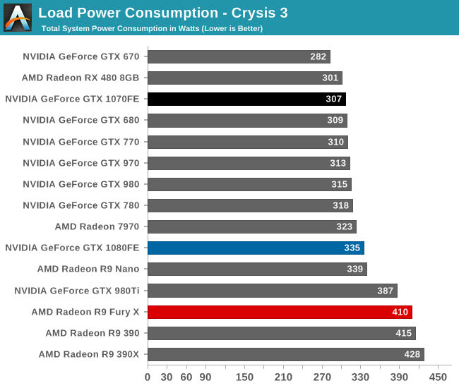
I always thought that nVidia's 8800 series that launched in 2006 was the best GPU series in their history. The 8800 GTX brought leaps and bounds in performance. It wasn't until June of 2008 that ATI had a GPU that could beat the 8800 GTX with the release of HD 4850/HD 4870. That means nVidia held the lead with a single generation for a year and half. Maxwell was good but AMD already had the R9 290X that was as good at the GTX 970 and it's refresh in June 2015, 9 month's after Maxwell's release was good enough to compete with the 970 and 980 with the R9 390 and 390X. But judging by what has come out of the performance number of the RX Vega 64, it will supposedly be as good as the GTX 1080 but not better than it and the 1080 Ti will still reign supreme. The GTX 1080 was launched last year meaning that Vega RX will be 1 year late and will consume 100 Watts more. So, that means Pascal will reign supreme until next year until AMD releases Navi in 2018. That's almost two years with nVidia being on top with Pascal. I don't think nVidia had such a long time with a lead in the GPU industry. That's not to say that Vega RX will be bad ( I welcome the fact that AMD finally has something to compete in the high end), it's about how Pascal is compared to previous GPU's in nVidia's history vs the competition.

I think we can all thank the cuts in the GPU division that AMD's last CEO made back in 2011 and the subsequent departure of top rated graphics talent in the subsequent years.

When you include everything in terms of power, performance (maybe not price), but at least in terms of power and performance and the fact that nVidia was able to stick an entire Desktop GPU inside a laptop and get the same permanence as a Desktop for the first time in their history is indeed an engineering achievement.

So, I think Pascal is their best generation in nVidia's history. Agree?

See I am not a AMD fanboy. Created a nVidia thread. ;)

ReplyEditDelete
 • 
Avatar image for Xtasy26
Xtasy26

5582

Forum Posts

0

Wiki Points

0

Followers

Reviews: 53

User Lists: 0

#51 Xtasy26
Member since 2008 • 5582 Posts

@waahahah said:
@Xtasy26 said:

Well, I could make the same argument as that they held back the previous generation ie. "Maxwell" for parity's sake. Which would be untrue because Maxwell didn't have the power consumption and performance that was the same exact as their laptop counterparts. But whereas with Pascal they do hence my argument that this was their best generation in terms of power/performance NOT price.

No you couldn't. They could have lead with 960m and 970m without the m on the end as the architecture was still a huge improvement.

Pascal architecture isn't the thing that allowed them to get the power design down. What allowed them to do that was transferring to smaller node sizes. Thats not nvidia's tech or achievement. They have significant room for improvements with the die shrinkage.

Uh they had previously did die shrinks before on their older GPU's but they never was able to fit an entire desktop line onto their laptops. AMD also did a die shrink to 14nm but their laptop GPU's of Polaris are not the same as the desktop version.

Avatar image for waahahah
waahahah

2462

Forum Posts

0

Wiki Points

0

Followers

Reviews: 2

User Lists: 5

#52 waahahah
Member since 2014 • 2462 Posts

@Xtasy26 said:
@waahahah said:
@Xtasy26 said:

Well, I could make the same argument as that they held back the previous generation ie. "Maxwell" for parity's sake. Which would be untrue because Maxwell didn't have the power consumption and performance that was the same exact as their laptop counterparts. But whereas with Pascal they do hence my argument that this was their best generation in terms of power/performance NOT price.

No you couldn't. They could have lead with 960m and 970m without the m on the end as the architecture was still a huge improvement.

Pascal architecture isn't the thing that allowed them to get the power design down. What allowed them to do that was transferring to smaller node sizes. Thats not nvidia's tech or achievement. They have significant room for improvements with the die shrinkage.

Uh they had previously did die shrinks before on their older GPU's but they never was able to fit an entire desktop line onto their laptops. AMD also did a die shrink to 14nm but their laptop GPU's of Polaris are not the same as the desktop version.

And? That doesn't refute my point. Die shrinkage is what allows them to fit more and more on a single chip at a lower tdp. Your entirely missing my point though, the desktop variants are bigger beefier versions... they didn't make a bigger beefier version this time because they had enough performance bump at the mobile design that they didn't need to for this iteration.

Avatar image for ronvalencia
ronvalencia

29612

Forum Posts

0

Wiki Points

0

Followers

Reviews: 1

User Lists: 0

#53  Edited By ronvalencia
Member since 2008 • 29612 Posts

@Xtasy26 said:
@waahahah said:
@Xtasy26 said:

Well, I could make the same argument as that they held back the previous generation ie. "Maxwell" for parity's sake. Which would be untrue because Maxwell didn't have the power consumption and performance that was the same exact as their laptop counterparts. But whereas with Pascal they do hence my argument that this was their best generation in terms of power/performance NOT price.

No you couldn't. They could have lead with 960m and 970m without the m on the end as the architecture was still a huge improvement.

Pascal architecture isn't the thing that allowed them to get the power design down. What allowed them to do that was transferring to smaller node sizes. Thats not nvidia's tech or achievement. They have significant room for improvements with the die shrinkage.

Uh they had previously did die shrinks before on their older GPU's but they never was able to fit an entire desktop line onto their laptops. AMD also did a die shrink to 14nm but their laptop GPU's of Polaris are not the same as the desktop version.

https://www.notebookcheck.net/AMD-Radeon-RX-580-Laptop-GPU.215184.0.html

RX-580 mobile is similar to the desktop version i.e. full 36 CU. Mobile version has 1257 Mhz to 1340 Mhz boost mode.

The Polaris 20 is manufactured in an improved 14nm process (LPP+) for higher clock speeds and some power efficiency improvements in idle. NVIDIA has been using 16 nm LPP+ since Pascal.

Avatar image for napo_sp
napo_sp

649

Forum Posts

0

Wiki Points

0

Followers

Reviews: 0

User Lists: 0

#54 napo_sp
Member since 2006 • 649 Posts

nope, 8800GTX still the best in their history because it cemented their status as the king.

Avatar image for Xtasy26
Xtasy26

5582

Forum Posts

0

Wiki Points

0

Followers

Reviews: 53

User Lists: 0

#55  Edited By Xtasy26
Member since 2008 • 5582 Posts

@waahahah said:
@Xtasy26 said:

Well, I could make the same argument as that they held back the previous generation ie. "Maxwell" for parity's sake. Which would be untrue because Maxwell didn't have the power consumption and performance that was the same exact as their laptop counterparts. But whereas with Pascal they do hence my argument that this was their best generation in terms of power/performance NOT price.

No you couldn't. They could have lead with 960m and 970m without the m on the end as the architecture was still a huge improvement.

Pascal architecture isn't the thing that allowed them to get the power design down. What allowed them to do that was transferring to smaller node sizes. Thats not nvidia's tech or achievement. They have significant room for improvements with the die shrinkage.

AMD also transferred to smaller node sizes but the RX 5XX series Gaming Laptop performance isn't the same as their desktop counterparts unlike the GTX 1060 6GB. Previous generations of die shrinks never had the same equivalent laptop version as the desktop version. No GPU in the history of nVidia had this great power/performance as Pascal does.

Avatar image for waahahah
waahahah

2462

Forum Posts

0

Wiki Points

0

Followers

Reviews: 2

User Lists: 5

#56  Edited By waahahah
Member since 2014 • 2462 Posts

@Xtasy26 said:
@waahahah said:
@Xtasy26 said:

Well, I could make the same argument as that they held back the previous generation ie. "Maxwell" for parity's sake. Which would be untrue because Maxwell didn't have the power consumption and performance that was the same exact as their laptop counterparts. But whereas with Pascal they do hence my argument that this was their best generation in terms of power/performance NOT price.

No you couldn't. They could have lead with 960m and 970m without the m on the end as the architecture was still a huge improvement.

Pascal architecture isn't the thing that allowed them to get the power design down. What allowed them to do that was transferring to smaller node sizes. Thats not nvidia's tech or achievement. They have significant room for improvements with the die shrinkage.

AMD also transferred to smaller node sizes but the RX 5XX series Gaming Laptop performance isn't the same as their desktop counterparts unlike the GTX 1060 6GB. Previous generations of die shrinks never had the same equivalent laptop version as the desktop version. No GPU in the history of nVidia had this great power/performance as Pascal does.

Are you really this stupid.

AMD chose to make slightly different chips

NVIDIA chose parity instead of performance bumps for desktops because they are in the lead.

Its a choice, based on NVIDIA having a lead on tech and its choosing to stay just ahead of AMD instead of make big leaps. They can consistently queue performance upgrades to meet everything AMD responds with. They started with the 8800...

Avatar image for gamingpcgod
GamingPCGod

132

Forum Posts

0

Wiki Points

0

Followers

Reviews: 0

User Lists: 0

#57 GamingPCGod
Member since 2015 • 132 Posts

For laptop gamers, definitely. I have the Alienware 15 1060 6gb variant, and I am incredibly surprised by it's performance. For a long time, laptops were basically more expensive and portable consoles in terms of performance, but now they basically have the gaming capabilities of desktops, minus the CPU heating issues (My i7-7700HQ get's too hot sometimes). My 1060 NEVER get's north of 65 degrees, despite the fact that sometimes I do insane OC.

Avatar image for Xtasy26
Xtasy26

5582

Forum Posts

0

Wiki Points

0

Followers

Reviews: 53

User Lists: 0

#58  Edited By Xtasy26
Member since 2008 • 5582 Posts

@waahahah said:
@Xtasy26 said:
@waahahah said:
@Xtasy26 said:

Well, I could make the same argument as that they held back the previous generation ie. "Maxwell" for parity's sake. Which would be untrue because Maxwell didn't have the power consumption and performance that was the same exact as their laptop counterparts. But whereas with Pascal they do hence my argument that this was their best generation in terms of power/performance NOT price.

No you couldn't. They could have lead with 960m and 970m without the m on the end as the architecture was still a huge improvement.

Pascal architecture isn't the thing that allowed them to get the power design down. What allowed them to do that was transferring to smaller node sizes. Thats not nvidia's tech or achievement. They have significant room for improvements with the die shrinkage.

AMD also transferred to smaller node sizes but the RX 5XX series Gaming Laptop performance isn't the same as their desktop counterparts unlike the GTX 1060 6GB. Previous generations of die shrinks never had the same equivalent laptop version as the desktop version. No GPU in the history of nVidia had this great power/performance as Pascal does.

Are you really this stupid.

AMD chose to make slightly different chips

NVIDIA chose parity instead of performance bumps for desktops because they are in the lead.

Its a choice, based on NVIDIA having a lead on tech and its choosing to stay just ahead of AMD instead of make big leaps. They can consistently queue performance upgrades to meet everything AMD responds with. They started with the 8800...

Facepalm. I was arguing about your claim that nVidia's ability to put an entire desktop Pascal GPU inside a laptop was due to it going to 14nm, which is not the entire story. It was how well nVidia built the chip, with power consumption in mind as (me using an argument that AMD and both nVidia did die shrinks in previous generation going back 10+ years) never had were they able to put an entire desktop level GPU inside a laptop. nVidia as been focusing on power consumption over the last 4 - 5 years as told by nVidia's Graphics Architect Gary Tarolli (former 3DFX graphics chip architect). Looks like they finally perfected it 4 - 5 years later. Hence my argument that this is their best generation with respect to power/performance. And they didn't always have the best graphics card even post 8800 because AMD used dual graphics chip to counter nVidia's top end graphics cards ie the 4870 X2, HD 5970, HD 6990 and so on.

@gamingpcgod said:

For laptop gamers, definitely. I have the Alienware 15 1060 6gb variant, and I am incredibly surprised by it's performance. For a long time, laptops were basically more expensive and portable consoles in terms of performance, but now they basically have the gaming capabilities of desktops, minus the CPU heating issues (My i7-7700HQ get's too hot sometimes). My 1060 NEVER get's north of 65 degrees, despite the fact that sometimes I do insane OC.

Cool. I have the 17" version with the same processor and the 1060 6GB. How hot does your CPU get? I saw the GPU never reaching above 68 degrees Celsius.

Avatar image for waahahah
waahahah

2462

Forum Posts

0

Wiki Points

0

Followers

Reviews: 2

User Lists: 5

#59 waahahah
Member since 2014 • 2462 Posts

@Xtasy26 said:

Facepalm. I was arguing about your claim that nVidia's ability to put an entire desktop Pascal GPU inside a laptop was due to it going to 14nm, which is not the entire story. It was how well nVidia built the chip, with power consumption in mind as (me using an argument that AMD and both nVidia did die shrinks in previous generation going back 10+ years) never had were they able to put an entire desktop level GPU inside a laptop. nVidia as been focusing on power consumption over the last 4 - 5 years as told by nVidia's Graphics Architect Gary Tarolli (former 3DFX graphics chip architect). Looks like they finally perfected it 4 - 5 years later. Hence my argument that this is their best generation with respect to power/performance.

They are the same architectures. Your distinction is stupid because you believe there is no *laptop* version. What I'm saying is there is no *desktop* version explicitly. They took the laptop GPU and sense it still performs better than AMD's offering just stuck it in a desktop. NVIDIA's architecture has been better for quite some time. They've had more overhead any way so going to 14nm allowed them to get competitive performance with using the same chipset.

So yes, the 14nm allowed them to fit more into a laptop gpu.. along with their latest iteration of gpu tech. And the next gen is going to be again better. AMD's vega is still basically comparable with nvidias 10xx series offering... which gives nvidia the option to not worry about making a desktop counterpart, they can just stick with a laptop tdp design.

Avatar image for Xtasy26
Xtasy26

5582

Forum Posts

0

Wiki Points

0

Followers

Reviews: 53

User Lists: 0

#60 Xtasy26
Member since 2008 • 5582 Posts

@ronvalencia said:
@Xtasy26 said:
@waahahah said:
@Xtasy26 said:

Well, I could make the same argument as that they held back the previous generation ie. "Maxwell" for parity's sake. Which would be untrue because Maxwell didn't have the power consumption and performance that was the same exact as their laptop counterparts. But whereas with Pascal they do hence my argument that this was their best generation in terms of power/performance NOT price.

No you couldn't. They could have lead with 960m and 970m without the m on the end as the architecture was still a huge improvement.

Pascal architecture isn't the thing that allowed them to get the power design down. What allowed them to do that was transferring to smaller node sizes. Thats not nvidia's tech or achievement. They have significant room for improvements with the die shrinkage.

Uh they had previously did die shrinks before on their older GPU's but they never was able to fit an entire desktop line onto their laptops. AMD also did a die shrink to 14nm but their laptop GPU's of Polaris are not the same as the desktop version.

https://www.notebookcheck.net/AMD-Radeon-RX-580-Laptop-GPU.215184.0.html

RX-580 mobile is similar to the desktop version i.e. full 36 CU. Mobile version has 1257 Mhz to 1340 Mhz boost mode.

The Polaris 20 is manufactured in an improved 14nm process (LPP+) for higher clock speeds and some power efficiency improvements in idle. NVIDIA has been using 16 nm LPP+ since Pascal.

The laptop version of the GTX 1060 6GB beat's the laptop version of the RX 580 from preliminary benchmarks against the RX 580 (at least if TimeSpy benches were to be included).

In terms of Graphics Score the GTX 1060 6GB in TimeSpy gets 3,747.

http://techavenue.wixsite.com/techavenue/alienware-17-r4

With RX 580 you will get a Graphics score of 3375 in Time Spy.

https://www.youtube.com/watch?v=n4ZP6k9ThoY

Look at video part at 0:46. So, the GTX 1060 will be faster.

With the Alienware you could also use Alienware's proprietary Graphics Amplifier which connect's to PCI-Express 3.0 port and use an external graphics card so much more future proof.

Avatar image for gamingpcgod
GamingPCGod

132

Forum Posts

0

Wiki Points

0

Followers

Reviews: 0

User Lists: 0

#61  Edited By GamingPCGod
Member since 2015 • 132 Posts

@Xtasy26: On really heavy loads, (for example, BF4 with a 200% supersampling) it can get to 83 C spikes, but typically hovers around 76-80. However, most games it stays in the high 60s-low 70s.

What's funny is that despite the high temps, I have had no CPU related crashes, and the crashes I have had are due to too high GPU voltages during OC.

Avatar image for ronvalencia
ronvalencia

29612

Forum Posts

0

Wiki Points

0

Followers

Reviews: 1

User Lists: 0

#62  Edited By ronvalencia
Member since 2008 • 29612 Posts

@Xtasy26 said:
@ronvalencia said:
@Xtasy26 said:
@waahahah said:

No you couldn't. They could have lead with 960m and 970m without the m on the end as the architecture was still a huge improvement.

Pascal architecture isn't the thing that allowed them to get the power design down. What allowed them to do that was transferring to smaller node sizes. Thats not nvidia's tech or achievement. They have significant room for improvements with the die shrinkage.

Uh they had previously did die shrinks before on their older GPU's but they never was able to fit an entire desktop line onto their laptops. AMD also did a die shrink to 14nm but their laptop GPU's of Polaris are not the same as the desktop version.

https://www.notebookcheck.net/AMD-Radeon-RX-580-Laptop-GPU.215184.0.html

RX-580 mobile is similar to the desktop version i.e. full 36 CU. Mobile version has 1257 Mhz to 1340 Mhz boost mode.

The Polaris 20 is manufactured in an improved 14nm process (LPP+) for higher clock speeds and some power efficiency improvements in idle. NVIDIA has been using 16 nm LPP+ since Pascal.

The laptop version of the GTX 1060 6GB beat's the laptop version of the RX 580 from preliminary benchmarks against the RX 580 (at least if TimeSpy benches were to be included).

In terms of Graphics Score the GTX 1060 6GB in TimeSpy gets 3,747.

http://techavenue.wixsite.com/techavenue/alienware-17-r4

With RX 580 you will get a Graphics score of 3375 in Time Spy.

https://www.youtube.com/watch?v=n4ZP6k9ThoY

Look at video part at 0:46. So, the GTX 1060 will be faster.

With the Alienware you could also use Alienware's proprietary Graphics Amplifier which connect's to PCI-Express 3.0 port and use an external graphics card so much more future proof.

That's not my argument.

Alienware Graphics Amplifier utilizes four lanes of dedicated PCIe Gen 3. Normal desktop PC's PCI-E 3.0 slots has 16 lanes.

I'm done with fat gaming laptops and external GPUs.

Avatar image for waahahah
waahahah

2462

Forum Posts

0

Wiki Points

0

Followers

Reviews: 2

User Lists: 5

#63 waahahah
Member since 2014 • 2462 Posts

@Xtasy26 said:

The laptop version of the GTX 1060 6GB beat's the laptop version of the RX 580 from preliminary benchmarks against the RX 580 (at least if TimeSpy benches were to be included).

In terms of Graphics Score the GTX 1060 6GB in TimeSpy gets 3,747.

http://techavenue.wixsite.com/techavenue/alienware-17-r4

With RX 580 you will get a Graphics score of 3375 in Time Spy.

https://www.youtube.com/watch?v=n4ZP6k9ThoY

Look at video part at 0:46. So, the GTX 1060 will be faster.

With the Alienware you could also use Alienware's proprietary Graphics Amplifier which connect's to PCI-Express 3.0 port and use an external graphics card so much more future proof.

He's pointing out the 580 mobile chip is the same except for clock. Laptops do throttle because of heat.

Avatar image for Xtasy26
Xtasy26

5582

Forum Posts

0

Wiki Points

0

Followers

Reviews: 53

User Lists: 0

#64 Xtasy26
Member since 2008 • 5582 Posts

@waahahah said:
@Xtasy26 said:

Facepalm. I was arguing about your claim that nVidia's ability to put an entire desktop Pascal GPU inside a laptop was due to it going to 14nm, which is not the entire story. It was how well nVidia built the chip, with power consumption in mind as (me using an argument that AMD and both nVidia did die shrinks in previous generation going back 10+ years) never had were they able to put an entire desktop level GPU inside a laptop. nVidia as been focusing on power consumption over the last 4 - 5 years as told by nVidia's Graphics Architect Gary Tarolli (former 3DFX graphics chip architect). Looks like they finally perfected it 4 - 5 years later. Hence my argument that this is their best generation with respect to power/performance.

They are the same architectures. Your distinction is stupid because you believe there is no *laptop* version. What I'm saying is there is no *desktop* version explicitly. They took the laptop GPU and sense it still performs better than AMD's offering just stuck it in a desktop. NVIDIA's architecture has been better for quite some time. They've had more overhead any way so going to 14nm allowed them to get competitive performance with using the same chipset.

So yes, the 14nm allowed them to fit more into a laptop gpu.. along with their latest iteration of gpu tech. And the next gen is going to be again better. AMD's vega is still basically comparable with nvidias 10xx series offering... which gives nvidia the option to not worry about making a desktop counterpart, they can just stick with a laptop tdp design.

All your spouting is speculation. There is no evidence that they took a "laptop" version and stuck inside a desktop. If you bothered to ever look at the event launch of Pascal nVidia's CEO specifically stated that they focused on power optimization on Pascal, it was so good that they were able to stick an entire desktop version inside an laptop. And this is not something new nVidia has been trying to cut down on power consumption on their desktop line going back 4+ years as noted by nVidia Graphics Archited Gary Tarolli, so no they were not focusing on "Laptop design" first they were always targeting the best possible desktop GPU they can make with the best power consumption. That has been nVidia's modus operandi since they learned their lesson from their Fermi generation.

Avatar image for waahahah
waahahah

2462

Forum Posts

0

Wiki Points

0

Followers

Reviews: 2

User Lists: 5

#65 waahahah
Member since 2014 • 2462 Posts

@Xtasy26 said:
@waahahah said:
@Xtasy26 said:

Facepalm. I was arguing about your claim that nVidia's ability to put an entire desktop Pascal GPU inside a laptop was due to it going to 14nm, which is not the entire story. It was how well nVidia built the chip, with power consumption in mind as (me using an argument that AMD and both nVidia did die shrinks in previous generation going back 10+ years) never had were they able to put an entire desktop level GPU inside a laptop. nVidia as been focusing on power consumption over the last 4 - 5 years as told by nVidia's Graphics Architect Gary Tarolli (former 3DFX graphics chip architect). Looks like they finally perfected it 4 - 5 years later. Hence my argument that this is their best generation with respect to power/performance.

They are the same architectures. Your distinction is stupid because you believe there is no *laptop* version. What I'm saying is there is no *desktop* version explicitly. They took the laptop GPU and sense it still performs better than AMD's offering just stuck it in a desktop. NVIDIA's architecture has been better for quite some time. They've had more overhead any way so going to 14nm allowed them to get competitive performance with using the same chipset.

So yes, the 14nm allowed them to fit more into a laptop gpu.. along with their latest iteration of gpu tech. And the next gen is going to be again better. AMD's vega is still basically comparable with nvidias 10xx series offering... which gives nvidia the option to not worry about making a desktop counterpart, they can just stick with a laptop tdp design.

All your spouting is speculation. There is no evidence that they took a "laptop" version and stuck inside a desktop. If you bothered to ever look at the event launch of Pascal nVidia's CEO specifically stated that they focused on power optimization on Pascal, it was so good that they were able to stick an entire desktop version inside an laptop. And this is not something new nVidia has been trying to cut down on power consumption on their desktop line going back 4+ years as noted by nVidia Graphics Archited Gary Tarolli, so no they were not focusing on "Laptop design" first they were always targeting the best possible desktop GPU they can make with the best power consumption. That has been nVidia's modus operandi since they learned their lesson from their Fermi generation.

There is evidence because they didn't need the performance they used laptop TDP design where they have room to raise the clock on the PC... instead of matching it because of better cooling. Many OC versions do this any way so your distinction is dumb.

Avatar image for ronvalencia
ronvalencia

29612

Forum Posts

0

Wiki Points

0

Followers

Reviews: 1

User Lists: 0

#66  Edited By ronvalencia
Member since 2008 • 29612 Posts

@Xtasy26 said:
@waahahah said:
@Xtasy26 said:

Facepalm. I was arguing about your claim that nVidia's ability to put an entire desktop Pascal GPU inside a laptop was due to it going to 14nm, which is not the entire story. It was how well nVidia built the chip, with power consumption in mind as (me using an argument that AMD and both nVidia did die shrinks in previous generation going back 10+ years) never had were they able to put an entire desktop level GPU inside a laptop. nVidia as been focusing on power consumption over the last 4 - 5 years as told by nVidia's Graphics Architect Gary Tarolli (former 3DFX graphics chip architect). Looks like they finally perfected it 4 - 5 years later. Hence my argument that this is their best generation with respect to power/performance.

They are the same architectures. Your distinction is stupid because you believe there is no *laptop* version. What I'm saying is there is no *desktop* version explicitly. They took the laptop GPU and sense it still performs better than AMD's offering just stuck it in a desktop. NVIDIA's architecture has been better for quite some time. They've had more overhead any way so going to 14nm allowed them to get competitive performance with using the same chipset.

So yes, the 14nm allowed them to fit more into a laptop gpu.. along with their latest iteration of gpu tech. And the next gen is going to be again better. AMD's vega is still basically comparable with nvidias 10xx series offering... which gives nvidia the option to not worry about making a desktop counterpart, they can just stick with a laptop tdp design.

All your spouting is speculation. There is no evidence that they took a "laptop" version and stuck inside a desktop. If you bothered to ever look at the event launch of Pascal nVidia's CEO specifically stated that they focused on power optimization on Pascal, it was so good that they were able to stick an entire desktop version inside an laptop. And this is not something new nVidia has been trying to cut down on power consumption on their desktop line going back 4+ years as noted by nVidia Graphics Archited Gary Tarolli, so no they were not focusing on "Laptop design" first they were always targeting the best possible desktop GPU they can make with the best power consumption. That has been nVidia's modus operandi since they learned their lesson from their Fermi generation.

For AMD GPUs, mobile version are speed binned/low resistance/better yield desktop chips. Low resistance = lower voltage, hence less power consumption.

VEGA 11 is the VEGA SKU to replace RX-580 SKUs.

My 7770 GPU aka 8870M aka R9-M270 series has about half the power consumption from the desktop 7770.

Avatar image for waahahah
waahahah

2462

Forum Posts

0

Wiki Points

0

Followers

Reviews: 2

User Lists: 5

#67  Edited By waahahah
Member since 2014 • 2462 Posts

@ronvalencia said:
@Xtasy26 said:
@waahahah said:
@Xtasy26 said:

Facepalm. I was arguing about your claim that nVidia's ability to put an entire desktop Pascal GPU inside a laptop was due to it going to 14nm, which is not the entire story. It was how well nVidia built the chip, with power consumption in mind as (me using an argument that AMD and both nVidia did die shrinks in previous generation going back 10+ years) never had were they able to put an entire desktop level GPU inside a laptop. nVidia as been focusing on power consumption over the last 4 - 5 years as told by nVidia's Graphics Architect Gary Tarolli (former 3DFX graphics chip architect). Looks like they finally perfected it 4 - 5 years later. Hence my argument that this is their best generation with respect to power/performance.

They are the same architectures. Your distinction is stupid because you believe there is no *laptop* version. What I'm saying is there is no *desktop* version explicitly. They took the laptop GPU and sense it still performs better than AMD's offering just stuck it in a desktop. NVIDIA's architecture has been better for quite some time. They've had more overhead any way so going to 14nm allowed them to get competitive performance with using the same chipset.

So yes, the 14nm allowed them to fit more into a laptop gpu.. along with their latest iteration of gpu tech. And the next gen is going to be again better. AMD's vega is still basically comparable with nvidias 10xx series offering... which gives nvidia the option to not worry about making a desktop counterpart, they can just stick with a laptop tdp design.

All your spouting is speculation. There is no evidence that they took a "laptop" version and stuck inside a desktop. If you bothered to ever look at the event launch of Pascal nVidia's CEO specifically stated that they focused on power optimization on Pascal, it was so good that they were able to stick an entire desktop version inside an laptop. And this is not something new nVidia has been trying to cut down on power consumption on their desktop line going back 4+ years as noted by nVidia Graphics Archited Gary Tarolli, so no they were not focusing on "Laptop design" first they were always targeting the best possible desktop GPU they can make with the best power consumption. That has been nVidia's modus operandi since they learned their lesson from their Fermi generation.

For AMD GPUs, mobile version are speed binned/low resistance/better yield desktop chips. Low resistance = lower voltage, hence less power consumption.

VEGA 11 is the VEGA SKU to replace RX-580 SKUs.

My 7770 GPU aka 8870M aka R9-270 series has about half the power consumption from the desktop 7770.

oh so its not just node, but material (neither have anything to do with architecture)

Avatar image for ronvalencia
ronvalencia

29612

Forum Posts

0

Wiki Points

0

Followers

Reviews: 1

User Lists: 0

#68  Edited By ronvalencia
Member since 2008 • 29612 Posts

@waahahah said:
@ronvalencia said:
@Xtasy26 said:
@waahahah said:

They are the same architectures. Your distinction is stupid because you believe there is no *laptop* version. What I'm saying is there is no *desktop* version explicitly. They took the laptop GPU and sense it still performs better than AMD's offering just stuck it in a desktop. NVIDIA's architecture has been better for quite some time. They've had more overhead any way so going to 14nm allowed them to get competitive performance with using the same chipset.

So yes, the 14nm allowed them to fit more into a laptop gpu.. along with their latest iteration of gpu tech. And the next gen is going to be again better. AMD's vega is still basically comparable with nvidias 10xx series offering... which gives nvidia the option to not worry about making a desktop counterpart, they can just stick with a laptop tdp design.

All your spouting is speculation. There is no evidence that they took a "laptop" version and stuck inside a desktop. If you bothered to ever look at the event launch of Pascal nVidia's CEO specifically stated that they focused on power optimization on Pascal, it was so good that they were able to stick an entire desktop version inside an laptop. And this is not something new nVidia has been trying to cut down on power consumption on their desktop line going back 4+ years as noted by nVidia Graphics Archited Gary Tarolli, so no they were not focusing on "Laptop design" first they were always targeting the best possible desktop GPU they can make with the best power consumption. That has been nVidia's modus operandi since they learned their lesson from their Fermi generation.

For AMD GPUs, mobile version are speed binned/low resistance/better yield desktop chips. Low resistance = lower voltage, hence less power consumption.

VEGA 11 is the VEGA SKU to replace RX-580 SKUs.

My 7770 GPU aka 8870M aka R9-270 series has about half the power consumption from the desktop 7770.

oh so its not just node, but material (neither have anything to do with architecture)

My old 8870M/R9-M270 is just a lower resistance version from desktop 7770. Each manufactured chip has different electrical properties with the best yield chip having low resistance.

The problem with AMD GPU is DX11 driver which is still single thread for the command list and laptop CPUs has lower clock speeds.

If a laptop has a few CPU cores with lower clock speed, NVIDIA Pascal GPU is the better choice for DX11 based games.

Avatar image for waahahah
waahahah

2462

Forum Posts

0

Wiki Points

0

Followers

Reviews: 2

User Lists: 5

#69 waahahah
Member since 2014 • 2462 Posts

@ronvalencia said:

My old 8870M/R9-M270 is just a lower resistance version from desktop 7770. Each manufactured chip has different electrical properties with the best yield chip having low resistance.

The problem with AMD GPU is DX11 driver which is still single thread for the command list and laptop CPUs has lower clock speeds.

If a laptop has a few CPU cores with lower clock speed, NVIDIA Pascal GPU is the better choice for DX11 based games.

right different electrical proprieties usually is different materials, process, or node size.

Avatar image for ronvalencia
ronvalencia

29612

Forum Posts

0

Wiki Points

0

Followers

Reviews: 1

User Lists: 0

#70  Edited By ronvalencia
Member since 2008 • 29612 Posts

@waahahah said:
@ronvalencia said:

My old 8870M/R9-M270 is just a lower resistance version from desktop 7770. Each manufactured chip has different electrical properties with the best yield chip having low resistance.

The problem with AMD GPU is DX11 driver which is still single thread for the command list and laptop CPUs has lower clock speeds.

If a laptop has a few CPU cores with lower clock speed, NVIDIA Pascal GPU is the better choice for DX11 based games.

right different electrical proprieties usually is different materials, process, or node size.

It's manufacture quality with different chips e.g. the reason why some chips can tolerate lower voltage and why other chips can't handle it i.e. the "silicon lottery".

AMD already screened ultra low voltage capable chips for mobile chips.

Unlike Intel's desktop CPUs line, AMD is not screening desktop RX-580s into standard and low voltage SKU parts. AIBs might screen RX-580s with low voltage proprieties as super overclock version.

Avatar image for waahahah
waahahah

2462

Forum Posts

0

Wiki Points

0

Followers

Reviews: 2

User Lists: 5

#71 waahahah
Member since 2014 • 2462 Posts

@ronvalencia said:
@waahahah said:
@ronvalencia said:

My old 8870M/R9-M270 is just a lower resistance version from desktop 7770. Each manufactured chip has different electrical properties with the best yield chip having low resistance.

The problem with AMD GPU is DX11 driver which is still single thread for the command list and laptop CPUs has lower clock speeds.

If a laptop has a few CPU cores with lower clock speed, NVIDIA Pascal GPU is the better choice for DX11 based games.

right different electrical proprieties usually is different materials, process, or node size.

It's manufacture quality with different chips e.g. the reason why some chips can tolerate lower voltage and why other chips can't handle it i.e. the "silicon lottery".

AMD already screened low voltage capable chips for mobile chips.

so process, where nvidia's using a better process

Avatar image for ronvalencia
ronvalencia

29612

Forum Posts

0

Wiki Points

0

Followers

Reviews: 1

User Lists: 0

#72  Edited By ronvalencia
Member since 2008 • 29612 Posts

@waahahah said:
@ronvalencia said:
@waahahah said:
@ronvalencia said:

My old 8870M/R9-M270 is just a lower resistance version from desktop 7770. Each manufactured chip has different electrical properties with the best yield chip having low resistance.

The problem with AMD GPU is DX11 driver which is still single thread for the command list and laptop CPUs has lower clock speeds.

If a laptop has a few CPU cores with lower clock speed, NVIDIA Pascal GPU is the better choice for DX11 based games.

right different electrical proprieties usually is different materials, process, or node size.

It's manufacture quality with different chips e.g. the reason why some chips can tolerate lower voltage and why other chips can't handle it i.e. the "silicon lottery".

AMD already screened low voltage capable chips for mobile chips.

so process, where nvidia's using a better process

TSMC has two 16 nm FinFET versions i.e. FinFET and FinFET+ (second gen FinFET). NVIDIA used FinFET+ for Pascal.

https://www.extremetech.com/gaming/201417-nvidias-2016-roadmap-shows-huge-performance-gains-from-upcoming-pascal-architecture

Pascal is Nvidia’s follow-up to Maxwell, and the first desktop chip to use TSMC’s 16nmFF+ (FinFET+) process. This is the second-generation follow-up to TSMC’s first FinFET technology

GF has switch to 14 nm FinFET LLP+ (GF's second gen FinFET) during RX-580 generation.

Avatar image for Xtasy26
Xtasy26

5582

Forum Posts

0

Wiki Points

0

Followers

Reviews: 53

User Lists: 0

#73 Xtasy26
Member since 2008 • 5582 Posts

@ronvalencia said:
@Xtasy26 said:
@ronvalencia said:
@Xtasy26 said:
@waahahah said:

No you couldn't. They could have lead with 960m and 970m without the m on the end as the architecture was still a huge improvement.

Pascal architecture isn't the thing that allowed them to get the power design down. What allowed them to do that was transferring to smaller node sizes. Thats not nvidia's tech or achievement. They have significant room for improvements with the die shrinkage.

Uh they had previously did die shrinks before on their older GPU's but they never was able to fit an entire desktop line onto their laptops. AMD also did a die shrink to 14nm but their laptop GPU's of Polaris are not the same as the desktop version.

https://www.notebookcheck.net/AMD-Radeon-RX-580-Laptop-GPU.215184.0.html

RX-580 mobile is similar to the desktop version i.e. full 36 CU. Mobile version has 1257 Mhz to 1340 Mhz boost mode.

The Polaris 20 is manufactured in an improved 14nm process (LPP+) for higher clock speeds and some power efficiency improvements in idle. NVIDIA has been using 16 nm LPP+ since Pascal.

The laptop version of the GTX 1060 6GB beat's the laptop version of the RX 580 from preliminary benchmarks against the RX 580 (at least if TimeSpy benches were to be included).

In terms of Graphics Score the GTX 1060 6GB in TimeSpy gets 3,747.

http://techavenue.wixsite.com/techavenue/alienware-17-r4

With RX 580 you will get a Graphics score of 3375 in Time Spy.

https://www.youtube.com/watch?v=n4ZP6k9ThoY

Look at video part at 0:46. So, the GTX 1060 will be faster.

With the Alienware you could also use Alienware's proprietary Graphics Amplifier which connect's to PCI-Express 3.0 port and use an external graphics card so much more future proof.

That's not my argument.

Alienware Graphics Amplifier utilizes four lanes of dedicated PCIe Gen 3. Normal desktop PC's PCI-E 3.0 slots has 16 lanes.

I'm done with fat gaming laptops and external GPUs.

True. But depending on the game, sometimes there is slight hit. Not worth spending another $1,000+ on a 17" Gaming Laptop in the future when you get the Amplifier and new Graphics Card.

Avatar image for Xtasy26
Xtasy26

5582

Forum Posts

0

Wiki Points

0

Followers

Reviews: 53

User Lists: 0

#74 Xtasy26
Member since 2008 • 5582 Posts

@waahahah said:
@Xtasy26 said:
@waahahah said:
@Xtasy26 said:

Facepalm. I was arguing about your claim that nVidia's ability to put an entire desktop Pascal GPU inside a laptop was due to it going to 14nm, which is not the entire story. It was how well nVidia built the chip, with power consumption in mind as (me using an argument that AMD and both nVidia did die shrinks in previous generation going back 10+ years) never had were they able to put an entire desktop level GPU inside a laptop. nVidia as been focusing on power consumption over the last 4 - 5 years as told by nVidia's Graphics Architect Gary Tarolli (former 3DFX graphics chip architect). Looks like they finally perfected it 4 - 5 years later. Hence my argument that this is their best generation with respect to power/performance.

They are the same architectures. Your distinction is stupid because you believe there is no *laptop* version. What I'm saying is there is no *desktop* version explicitly. They took the laptop GPU and sense it still performs better than AMD's offering just stuck it in a desktop. NVIDIA's architecture has been better for quite some time. They've had more overhead any way so going to 14nm allowed them to get competitive performance with using the same chipset.

So yes, the 14nm allowed them to fit more into a laptop gpu.. along with their latest iteration of gpu tech. And the next gen is going to be again better. AMD's vega is still basically comparable with nvidias 10xx series offering... which gives nvidia the option to not worry about making a desktop counterpart, they can just stick with a laptop tdp design.

All your spouting is speculation. There is no evidence that they took a "laptop" version and stuck inside a desktop. If you bothered to ever look at the event launch of Pascal nVidia's CEO specifically stated that they focused on power optimization on Pascal, it was so good that they were able to stick an entire desktop version inside an laptop. And this is not something new nVidia has been trying to cut down on power consumption on their desktop line going back 4+ years as noted by nVidia Graphics Archited Gary Tarolli, so no they were not focusing on "Laptop design" first they were always targeting the best possible desktop GPU they can make with the best power consumption. That has been nVidia's modus operandi since they learned their lesson from their Fermi generation.

There is evidence because they didn't need the performance they used laptop TDP design where they have room to raise the clock on the PC... instead of matching it because of better cooling. Many OC versions do this any way so your distinction is dumb.

Baloney. No evidence as such that they used laptop TDP as a design basis. Where I have proof that they have been heavily focusing on power consumption going back to Maxwell. They just were damn good at power consumption and efficient architecture with Pascal. Hence my argument best power/performance ratio in their history.

Avatar image for waahahah
waahahah

2462

Forum Posts

0

Wiki Points

0

Followers

Reviews: 2

User Lists: 5

#75  Edited By waahahah
Member since 2014 • 2462 Posts

@Xtasy26 said:

Baloney. No evidence as such that they used laptop TDP as a design basis. Where I have proof that they have been heavily focusing on power consumption going back to Maxwell. They just were damn good at power consumption and efficient architecture with Pascal. Hence my argument best power/performance ratio in their history.

The fabrication technology including node size and node is the most notable thing that allowed both amd + nvidia to jump in power. Also nvidia is using better more power efficient nodes which allows them to be more efficient with die space. We already established LPP+ node fabs allow nvidia the parity option while ATI relies on die lottery, but ultimately uses the same chips..

And there is evidence they didn't make a version with more stream processors / clock targeted at a higher tdp... because it doesn't exist. That's evidence of them not making it. Like your not going to see a threadripper in a laptop any time soon with 16 cores because it'll cook the laptop. NVIDIA can sure as shit use its die space for power if it wanted to.

So apart from making a thread to say nvidia's best iteration of technology is its best... which is stating the obvious... this entire thread has no point.

Avatar image for Xtasy26
Xtasy26

5582

Forum Posts

0

Wiki Points

0

Followers

Reviews: 53

User Lists: 0

#76 Xtasy26
Member since 2008 • 5582 Posts

@waahahah said:
@Xtasy26 said:

Baloney. No evidence as such that they used laptop TDP as a design basis. Where I have proof that they have been heavily focusing on power consumption going back to Maxwell. They just were damn good at power consumption and efficient architecture with Pascal. Hence my argument best power/performance ratio in their history.

The fabrication technology including node size and node is the most notable thing that allowed both amd + nvidia to jump in power. Also nvidia is using better more power efficient nodes which allows them to be more efficient with die space. We already established LPP+ node fabs allow nvidia the parity option while ATI relies on die lottery, but ultimately uses the same chips..

And there is evidence they didn't make a version with more stream processors / clock targeted at a higher tdp... because it doesn't exist. That's evidence of them not making it. Like your not going to see a threadripper in a laptop any time soon with 16 cores because it'll cook the laptop. NVIDIA can sure as shit use its die space for power if it wanted to.

So apart from making a thread to say nvidia's best iteration of technology is its best... which is stating the obvious... this entire thread has no point.

Again, no where do you provide any proof that it was based off of laptop TDP. Where as there is plenty of proof coming from nVidia GPU architects where they heavily focused on TDP with Maxwell and with Pascal they reached sort of the "holy grail" of power consumption so much so that they were able to put an entire generation inside a laptop something that was unheard of before. If "node jump" was the main reasons than AMD would have been able to put an entire stack of Polaris GPU inside the laptop that was the same the same as the desktop version. As the RX 580 on the laptop is not the same as the RX 580 on the desktop. I could hit 1900 Mhz+ boost clock on my GTX 1060 that is as good as the Desktop GTX 1060 which can reach over 1900 Mhz+, I know this because my buddy has a EVGA GTX 1060 6GB and he is able to reach that frequency range. Even with the "silicon lottery" good luck trying to get a RX 580 laptop to hit the frequency range of the Desktop RX 580 lol.

Avatar image for waahahah
waahahah

2462

Forum Posts

0

Wiki Points

0

Followers

Reviews: 2

User Lists: 5

#77  Edited By waahahah
Member since 2014 • 2462 Posts

@Xtasy26 said:
@waahahah said:
@Xtasy26 said:

Baloney. No evidence as such that they used laptop TDP as a design basis. Where I have proof that they have been heavily focusing on power consumption going back to Maxwell. They just were damn good at power consumption and efficient architecture with Pascal. Hence my argument best power/performance ratio in their history.

The fabrication technology including node size and node is the most notable thing that allowed both amd + nvidia to jump in power. Also nvidia is using better more power efficient nodes which allows them to be more efficient with die space. We already established LPP+ node fabs allow nvidia the parity option while ATI relies on die lottery, but ultimately uses the same chips..

And there is evidence they didn't make a version with more stream processors / clock targeted at a higher tdp... because it doesn't exist. That's evidence of them not making it. Like your not going to see a threadripper in a laptop any time soon with 16 cores because it'll cook the laptop. NVIDIA can sure as shit use its die space for power if it wanted to.

So apart from making a thread to say nvidia's best iteration of technology is its best... which is stating the obvious... this entire thread has no point.

Again, no where do you provide any proof that it was based off of laptop TDP. Where as there is plenty of proof coming from nVidia GPU architects where they heavily focused on TDP with Maxwell and with Pascal they reached sort of the "holy grail" of power consumption so much so that they were able to put an entire generation inside a laptop something that was unheard of before. If "node jump" was the main reasons than AMD would have been able to put an entire stack of Polaris GPU inside the laptop that was the same the same as the desktop version. As the RX 580 on the laptop is not the same as the RX 580 on the desktop. I could hit 1900 Mhz+ boost clock on my GTX 1060 that is as good as the Desktop GTX 1060 which can reach over 1900 Mhz+, I know this because my buddy has a EVGA GTX 1060 6GB and he is able to reach that frequency range. Even with the "silicon lottery" good luck trying to get a RX 580 laptop to hit the frequency range of the Desktop RX 580 lol.

You half witted cretin, its pretty self evident that if it fits in a laptop, its tdp is designed for a laptop. Your still ignoring the fact that NVIDIA is using lpp+ fabrication wich has improved power design over what amd is using.

its pretty obvious they are leading in technology even before this iteration so they didn't need to make a beefier version specifically to outclass AMD on the desktop.

So apart from this is the latest iteration, you have no real point. They've had a lead in architecture since 8800... This is their latest and greatest variant because its their latest and greatest variant which is expected. Your measure of its the greatest because it fit in a laptop is basicaly arbitrary and random measure of success, and its not all tied to the architecture, some of it is tied to better thermal design in laptops, some of its designed to fabrication process, some of its tied to the architecture. Many technologies made this possible. AMD is still a little behind as they are not using the latest in fabrication techniques.

Avatar image for appariti0n
appariti0n

5013

Forum Posts

0

Wiki Points

0

Followers

Reviews: 1

User Lists: 0

#78 appariti0n
Member since 2009 • 5013 Posts

@waahahah: Doesn't mean it was "designed" for a laptop. Had they cut the die size of the 8800gtx by say 30%, it would have also been able to fit in a laptop with little to no modifications, and would have still been nearly double the performance of the 7900 which preceded it.

I'm wagering that they could have made the pascal chips bigger and even faster, there simply was no reason to. They were already so far ahead of AMD, it would have been pointless.

Avatar image for waahahah
waahahah

2462

Forum Posts

0

Wiki Points

0

Followers

Reviews: 2

User Lists: 5

#79 waahahah
Member since 2014 • 2462 Posts

@appariti0n said:

@waahahah: Doesn't mean it was "designed" for a laptop. Had they cut the die size of the 8800gtx by say 30%, it would have also been able to fit in a laptop with little to no modifications, and would have still been nearly double the performance of the 7900 which preceded it.

I'm wagering that they could have made the pascal chips bigger and even faster, there simply was no reason to. They were already so far ahead of AMD, it would have been pointless.

A. Having a target TDP lower than normal means its designed for a lower TDP, which so happens is a requirement for laptops and slate pcs. Its semantics at this point as the target TDP was definitely not designed for desktops... it was designed for mobile/laptops. Just look at the nvidia tegra tech... that wouldn't be possible if that wasn't their focus. And I'm pointing out this was enabled by node shrinkage as well as fabrication process as well as architecture and their lead over AMD. Again AMD has never really hit back very hard since the 8800.

B. I already pointed out they didn't bother making better/bigger chips. Its the basis of my argument that they have been ahead of AMD that they targeted a lower TDP instead of raw power. It might have been cheaper for them since they can make 1 chip and call it a day. AMD has to test all of their chips.

Avatar image for Xtasy26
Xtasy26

5582

Forum Posts

0

Wiki Points

0

Followers

Reviews: 53

User Lists: 0

#80 Xtasy26
Member since 2008 • 5582 Posts

@waahahah said:
@Xtasy26 said:
@waahahah said:
@Xtasy26 said:

Baloney. No evidence as such that they used laptop TDP as a design basis. Where I have proof that they have been heavily focusing on power consumption going back to Maxwell. They just were damn good at power consumption and efficient architecture with Pascal. Hence my argument best power/performance ratio in their history.

The fabrication technology including node size and node is the most notable thing that allowed both amd + nvidia to jump in power. Also nvidia is using better more power efficient nodes which allows them to be more efficient with die space. We already established LPP+ node fabs allow nvidia the parity option while ATI relies on die lottery, but ultimately uses the same chips..

And there is evidence they didn't make a version with more stream processors / clock targeted at a higher tdp... because it doesn't exist. That's evidence of them not making it. Like your not going to see a threadripper in a laptop any time soon with 16 cores because it'll cook the laptop. NVIDIA can sure as shit use its die space for power if it wanted to.

So apart from making a thread to say nvidia's best iteration of technology is its best... which is stating the obvious... this entire thread has no point.

Again, no where do you provide any proof that it was based off of laptop TDP. Where as there is plenty of proof coming from nVidia GPU architects where they heavily focused on TDP with Maxwell and with Pascal they reached sort of the "holy grail" of power consumption so much so that they were able to put an entire generation inside a laptop something that was unheard of before. If "node jump" was the main reasons than AMD would have been able to put an entire stack of Polaris GPU inside the laptop that was the same the same as the desktop version. As the RX 580 on the laptop is not the same as the RX 580 on the desktop. I could hit 1900 Mhz+ boost clock on my GTX 1060 that is as good as the Desktop GTX 1060 which can reach over 1900 Mhz+, I know this because my buddy has a EVGA GTX 1060 6GB and he is able to reach that frequency range. Even with the "silicon lottery" good luck trying to get a RX 580 laptop to hit the frequency range of the Desktop RX 580 lol.

You half witted cretin, its pretty self evident that if it fits in a laptop, its tdp is designed for a laptop. Your still ignoring the fact that NVIDIA is using lpp+ fabrication wich has improved power design over what amd is using.

its pretty obvious they are leading in technology even before this iteration so they didn't need to make a beefier version specifically to outclass AMD on the desktop.

So apart from this is the latest iteration, you have no real point. They've had a lead in architecture since 8800... This is their latest and greatest variant because its their latest and greatest variant which is expected. Your measure of its the greatest because it fit in a laptop is basicaly arbitrary and random measure of success, and its not all tied to the architecture, some of it is tied to better thermal design in laptops, some of its designed to fabrication process, some of its tied to the architecture. Many technologies made this possible. AMD is still a little behind as they are not using the latest in fabrication techniques.

You are the one who came up with the idiotic claim that they designed it with Laptop TDP which no one has been able to verify. Pulling something out of your behind. Where I have evidence where AMD's GPU architects telling that they focused on Power efficiency going back to Maxwell. Even in nVidia's Pascal launch event the CEO talked about going through traces in the circuit to make it as efficient as possible. You would know this if you actually watched the Pascal launch event and even listen to actual nVidia architects. So, your claim that they designed with Laptop TDP is a bunch of BS. Going on a new node doesn't automatically mean that it will allow them to make it power efficient to put an entire desktop class GPU inside the laptop, there are a lot of other factors like design, circuit optimization which nVidia talked about.

@waahahah said:
@appariti0n said:

@waahahah: Doesn't mean it was "designed" for a laptop. Had they cut the die size of the 8800gtx by say 30%, it would have also been able to fit in a laptop with little to no modifications, and would have still been nearly double the performance of the 7900 which preceded it.

I'm wagering that they could have made the pascal chips bigger and even faster, there simply was no reason to. They were already so far ahead of AMD, it would have been pointless.

A. Having a target TDP lower than normal means its designed for a lower TDP, which so happens is a requirement for laptops and slate pcs. Its semantics at this point as the target TDP was definitely not designed for desktops... it was designed for mobile/laptops. Just look at the nvidia tegra tech... that wouldn't be possible if that wasn't their focus. And I'm pointing out this was enabled by node shrinkage as well as fabrication process as well as architecture and their lead over AMD. Again AMD has never really hit back very hard since the 8800.

B. I already pointed out they didn't bother making better/bigger chips. Its the basis of my argument that they have been ahead of AMD that they targeted a lower TDP instead of raw power. It might have been cheaper for them since they can make 1 chip and call it a day. AMD has to test all of their chips.

LMAO, Tegra was designed for Handheld mobile devices and for their Car infotainment system. It was not targeted towards desktop where as Pascal was targeted towards Desktops with focus on power consumption. nVidia hit a gold mine with Maxwell architecture which eventually led to Pascal with it's best power/performance ratio in their history.

LOL, at AMD not really hitting back very hard since 8800 series. Tells me you are clueless about the GPU industry. The 4800 series and the 5800 series hit nVidia pretty hard. LMAO.

Avatar image for ronvalencia
ronvalencia

29612

Forum Posts

0

Wiki Points

0

Followers

Reviews: 1

User Lists: 0

#81  Edited By ronvalencia
Member since 2008 • 29612 Posts

@Xtasy26 said:
@waahahah said:
@Xtasy26 said:
@waahahah said:

The fabrication technology including node size and node is the most notable thing that allowed both amd + nvidia to jump in power. Also nvidia is using better more power efficient nodes which allows them to be more efficient with die space. We already established LPP+ node fabs allow nvidia the parity option while ATI relies on die lottery, but ultimately uses the same chips..

And there is evidence they didn't make a version with more stream processors / clock targeted at a higher tdp... because it doesn't exist. That's evidence of them not making it. Like your not going to see a threadripper in a laptop any time soon with 16 cores because it'll cook the laptop. NVIDIA can sure as shit use its die space for power if it wanted to.

So apart from making a thread to say nvidia's best iteration of technology is its best... which is stating the obvious... this entire thread has no point.

Again, no where do you provide any proof that it was based off of laptop TDP. Where as there is plenty of proof coming from nVidia GPU architects where they heavily focused on TDP with Maxwell and with Pascal they reached sort of the "holy grail" of power consumption so much so that they were able to put an entire generation inside a laptop something that was unheard of before. If "node jump" was the main reasons than AMD would have been able to put an entire stack of Polaris GPU inside the laptop that was the same the same as the desktop version. As the RX 580 on the laptop is not the same as the RX 580 on the desktop. I could hit 1900 Mhz+ boost clock on my GTX 1060 that is as good as the Desktop GTX 1060 which can reach over 1900 Mhz+, I know this because my buddy has a EVGA GTX 1060 6GB and he is able to reach that frequency range. Even with the "silicon lottery" good luck trying to get a RX 580 laptop to hit the frequency range of the Desktop RX 580 lol.

You half witted cretin, its pretty self evident that if it fits in a laptop, its tdp is designed for a laptop. Your still ignoring the fact that NVIDIA is using lpp+ fabrication wich has improved power design over what amd is using.

its pretty obvious they are leading in technology even before this iteration so they didn't need to make a beefier version specifically to outclass AMD on the desktop.

So apart from this is the latest iteration, you have no real point. They've had a lead in architecture since 8800... This is their latest and greatest variant because its their latest and greatest variant which is expected. Your measure of its the greatest because it fit in a laptop is basicaly arbitrary and random measure of success, and its not all tied to the architecture, some of it is tied to better thermal design in laptops, some of its designed to fabrication process, some of its tied to the architecture. Many technologies made this possible. AMD is still a little behind as they are not using the latest in fabrication techniques.

You are the one who came up with the idiotic claim that they designed it with Laptop TDP which no one has been able to verify. Pulling something out of your behind. Where I have evidence where AMD's GPU architects telling that they focused on Power efficiency going back to Maxwell. Even in nVidia's Pascal launch event the CEO talked about going through traces in the circuit to make it as efficient as possible. You would know this if you actually watched the Pascal launch event and even listen to actual nVidia architects. So, your claim that they designed with Laptop TDP is a bunch of BS. Going on a new node doesn't automatically mean that it will allow them to make it power efficient to put an entire desktop class GPU inside the laptop, there are a lot of other factors like design, circuit optimization which nVidia talked about.

@waahahah said:
@appariti0n said:

@waahahah: Doesn't mean it was "designed" for a laptop. Had they cut the die size of the 8800gtx by say 30%, it would have also been able to fit in a laptop with little to no modifications, and would have still been nearly double the performance of the 7900 which preceded it.

I'm wagering that they could have made the pascal chips bigger and even faster, there simply was no reason to. They were already so far ahead of AMD, it would have been pointless.

A. Having a target TDP lower than normal means its designed for a lower TDP, which so happens is a requirement for laptops and slate pcs. Its semantics at this point as the target TDP was definitely not designed for desktops... it was designed for mobile/laptops. Just look at the nvidia tegra tech... that wouldn't be possible if that wasn't their focus. And I'm pointing out this was enabled by node shrinkage as well as fabrication process as well as architecture and their lead over AMD. Again AMD has never really hit back very hard since the 8800.

B. I already pointed out they didn't bother making better/bigger chips. Its the basis of my argument that they have been ahead of AMD that they targeted a lower TDP instead of raw power. It might have been cheaper for them since they can make 1 chip and call it a day. AMD has to test all of their chips.

LMAO, Tegra was designed for Handheld mobile devices and for their Car infotainment system. It was not targeted towards desktop where as Pascal was targeted towards Desktops with focus on power consumption. nVidia hit a gold mine with Maxwell architecture which eventually led to Pascal with it's best power/performance ratio in their history.

LOL, at AMD not really hitting back very hard since 8800 series. Tells me you are clueless about the GPU industry. The 4800 series and the 5800 series hit nVidia pretty hard. LMAO.

Maxwell has tile cache rendering advantage i.e. ROPS and TMU direct access to L2 cache.

Maxwell has DCC advantage.

Maxwell has rasterization scaling advantage.

Net result: Maxwell has graphics pipeline advantage. The core business why NVIDIA is in the GPU business not playing with DSP business.

AMD GPUs are more DSP than GPU i.e. weaker graphics pipeline hardware with plenty of compute TFLOPS.

Avatar image for appariti0n
appariti0n

5013

Forum Posts

0

Wiki Points

0

Followers

Reviews: 1

User Lists: 0

#82 appariti0n
Member since 2009 • 5013 Posts

@Xtasy26: Yup, 4870 was great, as was the 5870. The 7970 was no slouch either.

It's really only since the gtx 780 that AMD has really started to fall behind again.

Avatar image for waahahah
waahahah

2462

Forum Posts

0

Wiki Points

0

Followers

Reviews: 2

User Lists: 5

#83  Edited By waahahah
Member since 2014 • 2462 Posts

@Xtasy26 said:

You are the one who came up with the idiotic claim that they designed it with Laptop TDP which no one has been able to verify. Pulling something out of your behind. Where I have evidence where AMD's GPU architects telling that they focused on Power efficiency going back to Maxwell. Even in nVidia's Pascal launch event the CEO talked about going through traces in the circuit to make it as efficient as possible. You would know this if you actually watched the Pascal launch event and even listen to actual nVidia architects. So, your claim that they designed with Laptop TDP is a bunch of BS. Going on a new node doesn't automatically mean that it will allow them to make it power efficient to put an entire desktop class GPU inside the laptop, there are a lot of other factors like design, circuit optimization which nVidia talked about.

Again its self evident... are you really this stupid?

LMAO, Tegra was designed for Handheld mobile devices and for their Car infotainment system. It was not targeted towards desktop where as Pascal was targeted towards Desktops with focus on power consumption. nVidia hit a gold mine with Maxwell architecture which eventually led to Pascal with it's best power/performance ratio in their history.

LOL, at AMD not really hitting back very hard since 8800 series. Tells me you are clueless about the GPU industry. The 4800 series and the 5800 series hit nVidia pretty hard. LMAO.

You are this stupid. Your statement makes me believe you think tegra is a gpu architecture? Its not, Tegra... the latest tegra is a combined pascal + arm soc. Prior to that Tegra had a maxwell.. and at some point they started with a seperate ultra low power geforce. So they are targeting mobile/laptop spaces with their tdp. And there are many technologies that enable them to do this. One of the big ones is the node shrinkage and LPP+ fabrication.

So not only is it self evident that they targeted lower TDP's with their fabrication process and architecture... and they started targeting mobile with the inception of tegra. but there is actual evidence your trying to dismiss. They just shifted the design from laptop/pc variants to mobile/laptop variants and stuck the laptop TDP design in the desktop and called it 'good' because there isn't enough competition from AMD. They didn't NEED to make more powerful desktop version, they've had a lead over AMD so instead of making 3 variants... they stuck with 2. And they've been targeting mobile since the conception of tegra. They want to get in on the mobile market so their architectures have been designed for lower tdp's and node shrinkage have given them the ability to get the power they want at lower TDP targets as well as iterations of better architectures for power efficiency. There is a much larger handheld market then the desktop.

So again your post is pointless because its stating the obvious. NVIDIA's latest iteration of their GPU architecture is the best...

Avatar image for waahahah
waahahah

2462

Forum Posts

0

Wiki Points

0

Followers

Reviews: 2

User Lists: 5

#84  Edited By waahahah
Member since 2014 • 2462 Posts

@Xtasy26: I also don't think you understand how transistors work... better power saving technology will extend battery life while idle while keeping it a little cooler. The key word there is idle where it can disable power domains on a chip.

Having a chipped utilized to max on the other hand... heat generation and power usage is almost entirely based on fabrication, die size, and transistor count. The heat is generated during transistor switching because it basically is a short mid transition. Plus smaller node sizes mean it requires less voltage on the gates to switch so less idle power usage/current leakage it stays cooler while idle, and less power during switching. IE being able to put this much power in a TDP requirement for laptops is almost entirely based on fabrication process.

Avatar image for appariti0n
appariti0n

5013

Forum Posts

0

Wiki Points

0

Followers

Reviews: 1

User Lists: 0

#85  Edited By appariti0n
Member since 2009 • 5013 Posts

@waahahah: And yet the 780 ti, 980 ti, and 1080 ti each draw incrementally more power than the previous card under load.

If they were truly targetting lower TDP this time, the 1080 ti would draw less than the 780 ti/ 980 ti. Not more.

I also strongly suspect that intel is more the driving force behind being Nvidia being able to cram more powerful gpus into laptops. One must consider the TDP of not just the gpu, but the cpu as well, and Intel has made huge strides in this area.

Avatar image for waahahah
waahahah

2462

Forum Posts

0

Wiki Points

0

Followers

Reviews: 2

User Lists: 5

#86 waahahah
Member since 2014 • 2462 Posts

@appariti0n said:

@waahahah: And yet the 780 ti, 980 ti, and 1080 ti each draw incrementally more power than the previous card under load.

If they were truly targetting lower TDP this time, the 1080 ti would draw less than the 780 ti/ 980 ti. Not more.

I also strongly suspect that intel is more the driving force behind being Nvidia being able to cram more powerful gpus into laptops. One must consider the TDP of not just the gpu, but the cpu as well, and Intel has made huge strides in this area.

its also heat generation, you can cram more transistors in that generate less heat each, if you have a few million more, yes under load you'll still generate alot of heat. But you pointing out another aspect of this, if the 1080 generates more heat... its more likely to throttle in a laptop. But it still requires less V because of fabrication. Architecture won't change that. If it heats too much it will throttle more. But they might have thought its easier to stick a 1080 full version in just because it doesn't use the same power.

Also just bothering to look it up... laptops have slightly lower clock speeds but slightly more cuda cores for a 1070. @Xtasy26 I'm pretty sure your thread is incredibly pointless. NVIDIA even pointed out that its about 10% difference.

Avatar image for waahahah
waahahah

2462

Forum Posts

0

Wiki Points

0

Followers

Reviews: 2

User Lists: 5

#87 waahahah
Member since 2014 • 2462 Posts

@appariti0n said:

@waahahah: And yet the 780 ti, 980 ti, and 1080 ti each draw incrementally more power than the previous card under load.

If they were truly targetting lower TDP this time, the 1080 ti would draw less than the 780 ti/ 980 ti. Not more.

I also strongly suspect that intel is more the driving force behind being Nvidia being able to cram more powerful gpus into laptops. One must consider the TDP of not just the gpu, but the cpu as well, and Intel has made huge strides in this area.

Thats also dependent the laptop design. I had an MSI laptop with a 965m in it. It was designed to have a very small loop for the cpu/gpu. They were on seperate ends of the laptop, both had an exclusive intake vent and it vented upwards just above the keyboard. It also had a long vent connecting the two fans to allow heat to vent out. I imagine the heat between the cpu/gpu didn't affect each other that much. Thats how my alienware is right now but the vents are on the bottom and shoot out the back so I have to be careful to not block the vents.

Avatar image for Xtasy26
Xtasy26

5582

Forum Posts

0

Wiki Points

0

Followers

Reviews: 53

User Lists: 0

#88  Edited By Xtasy26
Member since 2008 • 5582 Posts

@waahahah said:
@Xtasy26 said:

You are the one who came up with the idiotic claim that they designed it with Laptop TDP which no one has been able to verify. Pulling something out of your behind. Where I have evidence where AMD's GPU architects telling that they focused on Power efficiency going back to Maxwell. Even in nVidia's Pascal launch event the CEO talked about going through traces in the circuit to make it as efficient as possible. You would know this if you actually watched the Pascal launch event and even listen to actual nVidia architects. So, your claim that they designed with Laptop TDP is a bunch of BS. Going on a new node doesn't automatically mean that it will allow them to make it power efficient to put an entire desktop class GPU inside the laptop, there are a lot of other factors like design, circuit optimization which nVidia talked about.

Again its self evident... are you really this stupid?

LMAO, Tegra was designed for Handheld mobile devices and for their Car infotainment system. It was not targeted towards desktop where as Pascal was targeted towards Desktops with focus on power consumption. nVidia hit a gold mine with Maxwell architecture which eventually led to Pascal with it's best power/performance ratio in their history.

LOL, at AMD not really hitting back very hard since 8800 series. Tells me you are clueless about the GPU industry. The 4800 series and the 5800 series hit nVidia pretty hard. LMAO.

You are this stupid. Your statement makes me believe you think tegra is a gpu architecture? Its not, Tegra... the latest tegra is a combined pascal + arm soc. Prior to that Tegra had a maxwell.. and at some point they started with a seperate ultra low power geforce. So they are targeting mobile/laptop spaces with their tdp. And there are many technologies that enable them to do this. One of the big ones is the node shrinkage and LPP+ fabrication.

So not only is it self evident that they targeted lower TDP's with their fabrication process and architecture... and they started targeting mobile with the inception of tegra. but there is actual evidence your trying to dismiss. They just shifted the design from laptop/pc variants to mobile/laptop variants and stuck the laptop TDP design in the desktop and called it 'good' because there isn't enough competition from AMD. They didn't NEED to make more powerful desktop version, they've had a lead over AMD so instead of making 3 variants... they stuck with 2. And they've been targeting mobile since the conception of tegra. They want to get in on the mobile market so their architectures have been designed for lower tdp's and node shrinkage have given them the ability to get the power they want at lower TDP targets as well as iterations of better architectures for power efficiency. There is a much larger handheld market then the desktop.

So again your post is pointless because its stating the obvious. NVIDIA's latest iteration of their GPU architecture is the best...

Facepalm. Did I say that they were targeting desktop with Tegra? Reading comprehension fail. I said Tegra was designed towards Handheld mobile devices. No where did I say Tegra is GPU architecture, stop putting words into my mouth. You are the one showing your stupidity by saying AMD not really hitting hard since 8800 series that tells me that you are clueless about the GPU industry as AMD was firing on all cylinders especially during 2008 - 2011 era prior to all these Graphics talent leaving and being laid off. Nowhere did I say that they were not targeting lower TDP's, I have been saying all along that they were heavily focusing on lower power at least per Maxwell and the reached the holy grail of power consumption with Pascal. You are regurgitating things I already stated.

Again you have to provide evidence they were targeting laptop TDP's with Pascal. I am saying what nVidia's CEO and GPU architects saying that they were focusing heavily on power consumption and they reached a point with Pascal with new node and circuit tweaking that they were finally able to reach power consumption level where they could put in an entire desktop class GPU inside a laptop.

Again, that goes to my point that you fail to read. That Pascal is their best generation with respect to power/performance.

@waahahah said:

@Xtasy26: I also don't think you understand how transistors work... better power saving technology will extend battery life while idle while keeping it a little cooler. The key word there is idle where it can disable power domains on a chip.

Having a chipped utilized to max on the other hand... heat generation and power usage is almost entirely based on fabrication, die size, and transistor count. The heat is generated during transistor switching because it basically is a short mid transition. Plus smaller node sizes mean it requires less voltage on the gates to switch so less idle power usage/current leakage it stays cooler while idle, and less power during switching. IE being able to put this much power in a TDP requirement for laptops is almost entirely based on fabrication process.

....And another pointless comment.

@waahahah said:
@appariti0n said:

@waahahah: And yet the 780 ti, 980 ti, and 1080 ti each draw incrementally more power than the previous card under load.

If they were truly targetting lower TDP this time, the 1080 ti would draw less than the 780 ti/ 980 ti. Not more.

I also strongly suspect that intel is more the driving force behind being Nvidia being able to cram more powerful gpus into laptops. One must consider the TDP of not just the gpu, but the cpu as well, and Intel has made huge strides in this area.

Also just bothering to look it up... laptops have slightly lower clock speeds but slightly more cuda cores for a 1070. @Xtasy26 I'm pretty sure your thread is incredibly pointless. NVIDIA even pointed out that its about 10% difference.

They said that it is within 10% difference. Doesn't mean it's always 10% as the boost clock depending on the Laptop manufacturer specs and their cooling you could get as good as desktop performance. Doesn't negate the fact what nVidia was able to do that with Pascal where they could get within that % range as the Desktop class is nothing short of amazing and thus makes Pascal their best generation with respect power/performance, hence my argument.

For example, I get boost clock well over 1900 MHz which is higher than boost clock of some Desktop GTX 1060's. Alienware has good cooling that getting higher boost clock can be achieved. I have not seen it higher than 68 C. This desktop level of performance is unheard of in previous generation of nVidia GPU's, the performance difference would be a lot more than "within 10%". If you have bothered to use Gaming Laptop's over the past 10+ years than you would know this. I had GTX 970M and it was no where near the performance of the desktop class GTX 970. That's why when I saw you could get desktop class GTX 1060 performance it was a no brainer to get the GTX 1060 laptop.

Avatar image for waahahah
waahahah

2462

Forum Posts

0

Wiki Points

0

Followers

Reviews: 2

User Lists: 5

#89  Edited By waahahah
Member since 2014 • 2462 Posts

@Xtasy26 said:

Facepalm. Did I say that they were targeting desktop with Tegra? Reading comprehension fail. I said Tegra was designed towards Handheld mobile devices. No where did I say Tegra is GPU architecture, stop putting words into my mouth. You are the one showing your stupidity by saying AMD not really hitting hard since 8800 series that tells me that you are clueless about the GPU industry as AMD was firing on all cylinders especially during 2008 - 2011 era prior to all these Graphics talent leaving and being laid off. Nowhere did I say that they were not targeting lower TDP's, I have been saying all along that they were heavily focusing on lower power at least per Maxwell and the reached the holy grail of power consumption with Pascal. You are regurgitating things I already stated.

Again you have to provide evidence they were targeting laptop TDP's with Pascal. I am saying what nVidia's CEO and GPU architects saying that they were focusing heavily on power consumption and they reached a point with Pascal with new node and circuit tweaking that they were finally able to reach power consumption level where they could put in an entire desktop class GPU inside a laptop.

Again, that goes to my point that you fail to read. That Pascal is their best generation with respect to power/performance.

Its a pascal, its the same architecture in tegra as the desktop... again your saying tegra like its a seperate gpu... This literally makes your assertion that there is no evidence that NVIDIA is targeting mobile/laptop space is literally wrong.

@Xtasy26 said:
@waahahah said:

@Xtasy26: I also don't think you understand how transistors work... better power saving technology will extend battery life while idle while keeping it a little cooler. The key word there is idle where it can disable power domains on a chip.

Having a chipped utilized to max on the other hand... heat generation and power usage is almost entirely based on fabrication, die size, and transistor count. The heat is generated during transistor switching because it basically is a short mid transition. Plus smaller node sizes mean it requires less voltage on the gates to switch so less idle power usage/current leakage it stays cooler while idle, and less power during switching. IE being able to put this much power in a TDP requirement for laptops is almost entirely based on fabrication process.

....And another pointless comment.

Just because you don't understand it... doesn't make it pointless. The fact is the node shrinkage and fabrication process is what allows them to fit this many transistors into a die space fit for a laptop. The node shrinkage is directly responsible for them not having to reduce functionality to fit in a laptop. They chose not to utilize more die space for desktops because they didn't need to.

They said that it is within 10% difference. Doesn't mean it's always 10% as the boost clock depending on the Laptop manufacturer specs and their cooling you could get as good as desktop performance.

For example, I get boost clock well over 1900 MHz which is higher than boost clock of some Desktop GTX 1060's. Alienware has good cooling that getting higher boost clock can be achieved. I have not seen it higher than 68 C. This desktop level of performance is unheard of in previous generation of nVidia GPU's, the performance difference would be a lot more than "within 10%". If you have bothered to use Gaming Laptop's over the years than you would know this. I had GTX 970M and it was no where near the performance of the desktop class GTX 970. That's why when I saw you could get desktop class GTX 1060 performance it was a no brainer to get the GTX 1060 laptop.

Did you read your argument against AMD using the same chips? You dismissed them because they are clocked differently. You are stupid.

I'd also like to clarify... I might have been wrong about the tdp, as @appariti0n pointed out that pascal uses more power. So the only thing that allows them to fit this many transistors into a laptop gpu comes down to the node shrinkage exclusively because the node shrinkage is the only thing that allows them to fit all those transistors into a particular die space.

edit: So again, your thread is entirely pointless, NVIDIA's best iteration is its best and with node shrinkage and the lack of AMD's competition they don't have a desktop class GPU because they didn't need to utilize additional die space. Thats the only thing that separates laptops from desktops... and its the thing that separates mobile from laptops... the size of the die is the bases of the different 'classes' of where you can fit the chip.

Avatar image for Xtasy26
Xtasy26

5582

Forum Posts

0

Wiki Points

0

Followers

Reviews: 53

User Lists: 0

#90  Edited By Xtasy26
Member since 2008 • 5582 Posts

@waahahah said:
@Xtasy26 said:

Facepalm. Did I say that they were targeting desktop with Tegra? Reading comprehension fail. I said Tegra was designed towards Handheld mobile devices. No where did I say Tegra is GPU architecture, stop putting words into my mouth. You are the one showing your stupidity by saying AMD not really hitting hard since 8800 series that tells me that you are clueless about the GPU industry as AMD was firing on all cylinders especially during 2008 - 2011 era prior to all these Graphics talent leaving and being laid off. Nowhere did I say that they were not targeting lower TDP's, I have been saying all along that they were heavily focusing on lower power at least per Maxwell and the reached the holy grail of power consumption with Pascal. You are regurgitating things I already stated.

Again you have to provide evidence they were targeting laptop TDP's with Pascal. I am saying what nVidia's CEO and GPU architects saying that they were focusing heavily on power consumption and they reached a point with Pascal with new node and circuit tweaking that they were finally able to reach power consumption level where they could put in an entire desktop class GPU inside a laptop.

Again, that goes to my point that you fail to read. That Pascal is their best generation with respect to power/performance.

Its a pascal, its the same architecture in tegra as the desktop... again your saying tegra like its a seperate gpu... This literally makes your assertion that there is no evidence that NVIDIA is targeting mobile/laptop space is literally wrong.

@Xtasy26 said:
@waahahah said:

@Xtasy26: I also don't think you understand how transistors work... better power saving technology will extend battery life while idle while keeping it a little cooler. The key word there is idle where it can disable power domains on a chip.

Having a chipped utilized to max on the other hand... heat generation and power usage is almost entirely based on fabrication, die size, and transistor count. The heat is generated during transistor switching because it basically is a short mid transition. Plus smaller node sizes mean it requires less voltage on the gates to switch so less idle power usage/current leakage it stays cooler while idle, and less power during switching. IE being able to put this much power in a TDP requirement for laptops is almost entirely based on fabrication process.

....And another pointless comment.

Just because you don't understand it... doesn't make it pointless. The fact is the node shrinkage and fabrication process is what allows them to fit this many transistors into a die space fit for a laptop. The node shrinkage is directly responsible for them not having to reduce functionality to fit in a laptop. They chose not to utilize more die space for desktops because they didn't need to.

They said that it is within 10% difference. Doesn't mean it's always 10% as the boost clock depending on the Laptop manufacturer specs and their cooling you could get as good as desktop performance.

For example, I get boost clock well over 1900 MHz which is higher than boost clock of some Desktop GTX 1060's. Alienware has good cooling that getting higher boost clock can be achieved. I have not seen it higher than 68 C. This desktop level of performance is unheard of in previous generation of nVidia GPU's, the performance difference would be a lot more than "within 10%". If you have bothered to use Gaming Laptop's over the years than you would know this. I had GTX 970M and it was no where near the performance of the desktop class GTX 970. That's why when I saw you could get desktop class GTX 1060 performance it was a no brainer to get the GTX 1060 laptop.

Did you read your argument against AMD using the same chips? You dismissed them because they are clocked differently. You are stupid.

I'd also like to clarify... I might have been wrong about the tdp, as @appariti0n pointed out that pascal uses more power. So the only thing that allows them to fit this many transistors into a laptop gpu comes down to the node shrinkage exclusively because the node shrinkage is the only thing that allows them to fit all those transistors into a particular die space.

edit: So again, your thread is entirely pointless, NVIDIA's best iteration is its best and with node shrinkage and the lack of AMD's competition they don't have a desktop class GPU because they didn't need to utilize additional die space. Thats the only thing that separates laptops from desktops... and its the thing that separates mobile from laptops... the size of the die is the bases of the different 'classes' of where you can fit the chip.

Never said anything about architecture with respect to Tegra other than it was geared towards mobile handheld devices. Stop putting words into my mouth.

I brought up AMD to argue against your stupid argument that it was only node shrinkage that was allowing them to reach TDP's that it did. Which is not the only reason. nVidia's focusing on power consumption with respect to the design of their GPU's as well as various other factors like optimization of the circuitry trace by trace as stated by nVidia CEO also played a role. To say otherwise would be downright idiotic. Gary Tarolli, GPU architect stated such, I would take his word over some clueless individual on a forum making arm chair analysis about power consumption only being the result of die shrinkage, which is downright stupid as even nVidia CEO and GPU architects mentioned as that being not the only reason.

If that was not the case then nVidia would have been able to fit an entire Maxwell GPU inside a laptop despite having similar power consumption as Pascal (under certain circumstances). That pretty much throws out your idiotic argument out the window tells me that you are clueless about GPU design. Even @appariti0n pointed this out to you but your too stupid to realize this.

Avatar image for waahahah
waahahah

2462

Forum Posts

0

Wiki Points

0

Followers

Reviews: 2

User Lists: 5

#91  Edited By waahahah
Member since 2014 • 2462 Posts

@Xtasy26 said:

Never said anything about architecture with respect to Tegra other than it was geared towards mobile handheld devices. Stop putting words into my mouth.

I know you didn't, I did, its evidence that the design of pascal is directly related to design for mobile space is not only self evident but... there is evidence. Your refutes against tegra make it seem like you don't understand that the design of tegra includes pascal...

I brought up AMD to argue against your stupid argument that it was only node shrinkage that was allowing them to reach TDP's that it did. Which is not the only reason. nVidia's focusing on power consumption with respect to the design of their GPU's as well as various other factors like optimization of the circuitry trace by trace as stated by nVidia CEO also played a role. To say otherwise would be downright idiotic. Gary Tarolli, GPU architect stated such, I would take his word over some clueless individual on a forum making arm chair analysis about power consumption only being the result of die shrinkage, which is downright stupid as even nVidia CEO and GPU architects mentioned as that being not the only reason.

But we also recently established that their TDP's aren't better... so their heat dissipation is directly related to laptop design and what allows them to fit it in their is die size. Which is directly related to the die shrinkage of this iteration.

If that was not the case then nVidia would have been able to fit an entire Maxwell GPU inside a laptop despite having similar power consumption as Pascal. That pretty much throws out your idiotic argument out the window tells me that you are clueless about GPU design. Even @appariti0n pointed this out to you but your too stupid to realize this.

Actually that fact makes it very literal that you are wrong. If they are using similar power consumption, what allows them to use it in a laptop is completely down to fabrication and die space. Your literally are wrong about the architecture being the important factor as it comes down to fabrication entirely. What allows them to have similar power consumption of the previous generation comes down to a combination of fabrication and optimization. But we just established power consumption isn't the limiting factor for a laptop when comparing maxwell and pascal. And the power consumption isn't the same... the pascal series as pointed out by @appariti0n its incrementally more...

So your thread is not only pointless it was based on a misconception that the architecture actually had enough gains that they could fit power into a lower TDP... thats not the case. They literally could fit the transistor count into a smaller die... which AMD is also doing. And you contradicting yourself when saying AMD isn't achieving since its not parity with the desktop's speed while NVIDIA also does not have parity with laptop/desktop specs. They are just a little closer.

I think we are done.

Avatar image for Xtasy26
Xtasy26

5582

Forum Posts

0

Wiki Points

0

Followers

Reviews: 53

User Lists: 0

#92  Edited By Xtasy26
Member since 2008 • 5582 Posts

@waahahah said:
@Xtasy26 said:

Never said anything about architecture with respect to Tegra other than it was geared towards mobile handheld devices. Stop putting words into my mouth.

I know you didn't, I did, its evidence that the design of pascal is directly related to design for mobile space is not only self evident but... there is evidence. Your refutes against tegra make it seem like you don't understand that the design of tegra includes pascal...

I brought up AMD to argue against your stupid argument that it was only node shrinkage that was allowing them to reach TDP's that it did. Which is not the only reason. nVidia's focusing on power consumption with respect to the design of their GPU's as well as various other factors like optimization of the circuitry trace by trace as stated by nVidia CEO also played a role. To say otherwise would be downright idiotic. Gary Tarolli, GPU architect stated such, I would take his word over some clueless individual on a forum making arm chair analysis about power consumption only being the result of die shrinkage, which is downright stupid as even nVidia CEO and GPU architects mentioned as that being not the only reason.

But we also recently established that their TDP's aren't better... so their heat dissipation is directly related to laptop design and what allows them to fit it in their is die size. Which is directly related to the die shrinkage of this iteration.

If that was not the case then nVidia would have been able to fit an entire Maxwell GPU inside a laptop despite having similar power consumption as Pascal. That pretty much throws out your idiotic argument out the window tells me that you are clueless about GPU design. Even @appariti0n pointed this out to you but your too stupid to realize this.

Actually that fact makes it very literal that you are wrong. If they are using similar power consumption, what allows them to use it in a laptop is completely down to fabrication and die space. Your literally are wrong about the architecture being the important factor as it comes down to fabrication entirely. What allows them to have similar power consumption of the previous generation comes down to a combination of fabrication and optimization. But we just established power consumption isn't the limiting factor for a laptop when comparing maxwell and pascal.

So your thread is not only pointless it was based on a misconception that the architecture actually had enough gains that they could fit power into a lower TDP... thats not the case. They literally could fit the transistor count into a smaller die... which AMD is also doing. And you contradicting yourself when saying AMD isn't achieving since its not parity with the desktop's speed while NVIDIA also does not have parity with laptop/desktop specs. They are just a little closer.

I think we are done.

Just stop. The more you talk the more fool you make of yourself. Yes, architecture and other factors do play a role in performance within a certain TDP or else Gary Tarolli one of the chief architects at nVidia would not be talking about it. nVidia is reaching close to parity with Pascal as their desktop counterparts unlike AMD. RX 580 on the laptop is far far behind the desktop counterparts. First of all, I am talking to a guy who didn't even own a GTX 970M and compared to a desktop class GTX 970, if you did you would know the performance difference is significant. I used to own a GTX 960 the 970M didn't even get the performance of a GTX 960 and a really nice GTX 960 would easily beat a 970M. It wouldn't be within 5% - 10% of the desktop class 970 whereas the GTX 1060 is and even some cases goes up to 1900 MHz+ boost clock which is higher than the boost clock of some desktop GTX 1060.

I knew you are an idiot when you claimed that Pascal was designed with "Laptop TDP" because if you bothered to look at power consumption you would see that GTX 1070 is only a couple of watts lower than a GTX 970.

Yet a laptop GTX 1070 would get a desktop level performance as the Desktop GTX 1070. Yet, a GTX 970M performs well below a desktop GTX 970 unlike the laptop GTX 1070 that's well within the threshold of the power brick even if you are exceeding. A 3W to 6W difference between a desktop 970 vs a GTX 1070 isn't going to make much of a difference when your Alienware 17" Gaming Laptop comes with a 280+ Watt power brick.

Yes, I think we are done here. We managed to figure out who the idiot was claiming that Pascal was designed with "Laptop TDP". LMAO.

Avatar image for waahahah
waahahah

2462

Forum Posts

0

Wiki Points

0

Followers

Reviews: 2

User Lists: 5

#93  Edited By waahahah
Member since 2014 • 2462 Posts

@Xtasy26 said:

Just stop. The more you talk the more fool you make of yourself. Yes, architecture and other factors do play a role in performance within a certain TDP or else Gary Tarolli one of the chief architects at nVidia would not be talking about it. nVidia is reaching close to parity with Pascal as their desktop counterparts unlike AMD. RX 580 on the laptop is far far behind the desktop counterparts. First of all, I am talking to a guy who didn't even own a GTX 970M and compared to a desktop class GTX 970, if you did you would know the performance difference is significant. I used to own a GTX 960 the 970M didn't even get the performance of a GTX 960 and a really nice GTX 960 would easily beat a 970M. It wouldn't be within 5% - 10% of the desktop class 970 whereas the GTX 1060 is and even some cases goes up to 1900 MHz+ boost clock which is higher than the boost clock of some desktop GTX 1060.

I knew you are an idiot when you claimed that Pascal was designed with "Laptop TDP" because if you bothered to look at power consumption you would see that GTX 1070 is only a couple of watts lower than a GTX 970.

Yet a laptop GTX 1070 would get a desktop level performance as the Desktop GTX 1070. Yet, a GTX 970M performs well below a desktop GTX 970 unlike the laptop GTX 1070 that's well within the threshold of the power brick even if you are exceeding. A 3W to 6W difference between a desktop 970 vs a GTX 1070 isn't going to make much of a difference when your Alienware 17" Gaming Laptop comes with 280 Watt power brick.

Yes, I think we are done here. We managed to figure out who the idiot was claiming that Pascal was designed with "Laptop TDP". LMAO.

ROLF you still don't get it, its the die space requirements that let them fit it in there... which is entirely based on fabrication. Yes I admitted I was wrong about the tdp target. But the fact that 1070 vs 980 is less than 10 watts... so its not a power requirement that makes them able to fit in in their, or architecture. Its entirely down to die size... I mean you proved yourself wrong at this point. Your literally proving that the limiting factor for laptops isn't power consumption...

So my initial assertion was right, this is ENTIRELY based on node shrinkage basically.

Also I wasn't really "wrong" about the tdp as I was pointing out that your assertion that the pascal improvements weren't targeted for laptops... which clearly they were targeted for mobile to fit into a tegra. So I'm actually right about that too. I was just wrong about the "tdp" aspect because I assumed it was lower because you were talking about how they 'fit' it in a laptop with power related optimizations.

IE there is no desktop class variant, there are mobile/laptop variants with room to grow because their target is for mobile markets. And this is just their best iteration and with no competition they don't need a larger desktop version with more cores or w/e.

Avatar image for appariti0n
appariti0n

5013

Forum Posts

0

Wiki Points

0

Followers

Reviews: 1

User Lists: 0

#94  Edited By appariti0n
Member since 2009 • 5013 Posts

Die size, fabrication, TDP, architecture, one can argue this stuff for days.

At the end of the day, it's easiest to simply compare the fastest single gpu card of each generation, and its relative performance.

780 ti vs 980 ti, 980 ti vs 1080 ti, etc.

Given that the 980 ti and 1080 ti have nearly identical TDP, it's especially valid.

So what was the performance increase from the 980 ti to the 1080 ti? 30%? 40? 50?

Unless it can hit well over a 100% increase, or more than double the performance, the 8800 GTX absolutely blows it out of the water. Case closed.

Avatar image for Xtasy26
Xtasy26

5582

Forum Posts

0

Wiki Points

0

Followers

Reviews: 53

User Lists: 0

#95  Edited By Xtasy26
Member since 2008 • 5582 Posts

@waahahah said:
@Xtasy26 said:

Just stop. The more you talk the more fool you make of yourself. Yes, architecture and other factors do play a role in performance within a certain TDP or else Gary Tarolli one of the chief architects at nVidia would not be talking about it. nVidia is reaching close to parity with Pascal as their desktop counterparts unlike AMD. RX 580 on the laptop is far far behind the desktop counterparts. First of all, I am talking to a guy who didn't even own a GTX 970M and compared to a desktop class GTX 970, if you did you would know the performance difference is significant. I used to own a GTX 960 the 970M didn't even get the performance of a GTX 960 and a really nice GTX 960 would easily beat a 970M. It wouldn't be within 5% - 10% of the desktop class 970 whereas the GTX 1060 is and even some cases goes up to 1900 MHz+ boost clock which is higher than the boost clock of some desktop GTX 1060.

I knew you are an idiot when you claimed that Pascal was designed with "Laptop TDP" because if you bothered to look at power consumption you would see that GTX 1070 is only a couple of watts lower than a GTX 970.

Yet a laptop GTX 1070 would get a desktop level performance as the Desktop GTX 1070. Yet, a GTX 970M performs well below a desktop GTX 970 unlike the laptop GTX 1070 that's well within the threshold of the power brick even if you are exceeding. A 3W to 6W difference between a desktop 970 vs a GTX 1070 isn't going to make much of a difference when your Alienware 17" Gaming Laptop comes with 280 Watt power brick.

Yes, I think we are done here. We managed to figure out who the idiot was claiming that Pascal was designed with "Laptop TDP". LMAO.

ROLF you still don't get it, its the die space requirements that let them fit it in there... which is entirely based on fabrication. Yes I admitted I was wrong about the tdp target. But the fact that 1070 vs 980 is less than 10 watts... so its not a power requirement that makes them able to fit in in their, or architecture. Its entirely down to die size... I mean you proved yourself wrong at this point. Your literally proving that the limiting factor for laptops isn't power consumption...

So my initial assertion was right, this is ENTIRELY based on node shrinkage basically.

Also I wasn't really "wrong" about the tdp as I was pointing out that your assertion that the pascal improvements weren't targeted for laptops... which clearly they were targeted for mobile to fit into a tegra. So I'm actually right about that too. I was just wrong about the "tdp" aspect because I assumed it was lower because you were talking about how they 'fit' it in a laptop with power related optimizations.

IE there is no desktop class variant, there are mobile/laptop variants with room to grow because their target is for mobile markets. And this is just their best iteration and with no competition they don't need a larger desktop version with more cores or w/e.

First of all, I never mentioned anything about die size. If you want to talk about it that is a totally different topic. Don't try to change the subject because you made a fool of yourself. I have said repeatedly there other factors like optimization of the circuit as noted to get the best performance with the best power consumption as stated by nVidia CEO during the Pascal launch. I just pointing your idiotic argument that Pascal was designed with "Laptop TDP".

"Your literally proving that the limiting factor for laptops isn't power consumption..."

No, s*** sherlock. As I have stated there other factors. Power consumption wasn't the only reason that they were able to fit a desktop class GPU inside a laptop with Pascal unlike Maxwell.

If you want to talk about die size, difference between 970 and 1070 is 84mm2. It will help nVidia's bottom line as they could make more on 300mm wafer. Bottom line nVidia did a great job with respect to it's ability to get the performance they did by their ability to put a desktop class GPU inside a laptop unlike any of their previous generations.

Avatar image for waahahah
waahahah

2462

Forum Posts

0

Wiki Points

0

Followers

Reviews: 2

User Lists: 5

#96  Edited By waahahah
Member since 2014 • 2462 Posts

@Xtasy26 said:

First of all, I never mentioned anything about die size. If you want to talk about it that is a totally different topic. Don't try to change the subject because you made a fool of yourself. I have said repeatedly there other factors like optimization of the circuit as noted to get the best performance with the best power consumption as stated by nVidia CEO during the Pascal launch. I just pointing your idiotic argument that Pascal was designed with "Laptop TDP".

You didn't I did. What the **** do you think shrinking the physical sizes will get you? A smaller micro chip. Which is my original assertion your arguing against. Your point is its more architecture, my point is its more fabrication.

"Your literally proving that the limiting factor for laptops isn't power consumption..."

No, s*** sherlock. As I have stated there other factors. Power consumption wasn't the only reason that they were able to fit a desktop class GPU inside a laptop with Pascal unlike Maxwell.

If you want to talk about die size, difference between 970 and 1070 is 84mm2. It will help nVidia's bottom line as they could make more on 300mm wafer. But size increase is not going make much of difference in terms of it's ability to fit inside a large 17" Alienware Gaming Laptop. nVidia did a great job with respect to it's ability to get the performance they did by their ability to put a desktop class GPU inside a laptop unlike any of their previous generations.

What is different from a laptop? Space and tdp. You have neither space or the power available you have to make a second variant of the chip. Like a 960m vs 960 is the 2x tdp design. 65 watt vs 120. Chipsize also matters when you consider limited space available on the board. If a 980 is the same power consumption as a 1070 than you proved power has nothing to do with the transition. Your entire argument that the architecture with the power savings is completely pointless, as it has nothing to do with being able to fit a desktop GPU into a laptop.

So that only leaves space left as a limited factor that NVIDIA has control over. If you really don't think that the die size matters then you have no ground to stand on. Because there would have been nothing stopping them sticking a 980 in a laptop with the same tdp and a slightly larger gpu. If that were true, the limiting factor probably had nothing to do with nvidia. Some technology allowed laptop manufacturers to use the desktop gpu instead of asking for a mobile variant of the chip.

A huge difference in clock/power consumption comes down to node shrinkage. Smaller transistors allow for faster switching, lower voltages, lower resistance (less heat generation), which is going to be the biggest factor when your under load. So they get a huge clock bump, huge power consumption drop under load and a smaller chip all based on node size. Two of which are hard requirements to get it into a laptop. The 28nm to 16nm is a huge factor in the performance bump.

Hell you can take a look at the specs and see that pascal is basically a maxwell with a few additionally features + a huge clock bump. That clock bump is likely due to the node shrinkage so the performance increase in large is due to the node shrink...

Also you can keep beating the "laptop tdp" drum. I worded somethings incorrectly but I'm not wrong that they are aiming for mobile markets with their last few iterations of geforce architecture. You still don't seem to understand the significance that they are dropping "desktop class" (a term as bad as 'laptop tdp') gpu's in favor of chips that can fit in mobile devices such as laptops... They are clearly targeting mobile devices. Its not only self evident but tegra is proof of that.

Avatar image for Xtasy26
Xtasy26

5582

Forum Posts

0

Wiki Points

0

Followers

Reviews: 53

User Lists: 0

#97  Edited By Xtasy26
Member since 2008 • 5582 Posts

@waahahah said:
@Xtasy26 said:

First of all, I never mentioned anything about die size. If you want to talk about it that is a totally different topic. Don't try to change the subject because you made a fool of yourself. I have said repeatedly there other factors like optimization of the circuit as noted to get the best performance with the best power consumption as stated by nVidia CEO during the Pascal launch. I just pointing your idiotic argument that Pascal was designed with "Laptop TDP".

You didn't I did. What the **** do you think shrinking the physical sizes will get you? A smaller micro chip. Which is my original assertion your arguing against. Your point is its more architecture, my point is its more fabrication.

"Your literally proving that the limiting factor for laptops isn't power consumption..."

No, s*** sherlock. As I have stated there other factors. Power consumption wasn't the only reason that they were able to fit a desktop class GPU inside a laptop with Pascal unlike Maxwell.

If you want to talk about die size, difference between 970 and 1070 is 84mm2. It will help nVidia's bottom line as they could make more on 300mm wafer. But size increase is not going make much of difference in terms of it's ability to fit inside a large 17" Alienware Gaming Laptop. nVidia did a great job with respect to it's ability to get the performance they did by their ability to put a desktop class GPU inside a laptop unlike any of their previous generations.

What is different from a laptop? Space and tdp. You have neither space or the power available you have to make a second variant of the chip. Like a 960m vs 960 is the 2x tdp design. 65 watt vs 120. Chipsize also matters when you consider limited space available on the board. If a 980 is the same power consumption as a 1070 than you proved power has nothing to do with the transition. Your entire argument that the architecture with the power savings is completely pointless, as it has nothing to do with being able to fit a desktop GPU into a laptop.

So that only leaves space left as a limited factor that NVIDIA has control over. If you really don't think that the die size matters then you have no ground to stand on. Because there would have been nothing stopping them sticking a 980 in a laptop with the same tdp and a slightly larger gpu. If that were true, the limiting factor probably had nothing to do with nvidia. Some technology allowed laptop manufacturers to use the desktop gpu instead of asking for a mobile variant of the chip.

A huge difference in clock/power consumption comes down to node shrinkage. Smaller transistors allow for faster switching, lower voltages, lower resistance (less heat generation), which is going to be the biggest factor when your under load. So they get a huge clock bump, huge power consumption drop under load and a smaller chip all based on node size. Two of which are hard requirements to get it into a laptop. The 28nm to 16nm is a huge factor in the performance bump.

Hell you can take a look at the specs and see that pascal is basically a maxwell with a few additionally features + a huge clock bump. That clock bump is likely due to the node shrinkage so the performance increase in large is due to the node shrink...

Also you can keep beating the "laptop tdp" drum. I worded somethings incorrectly but I'm not wrong that they are aiming for mobile markets with their last few iterations of geforce architecture. You still don't seem to understand the significance that they are dropping "desktop class" (a term as bad as 'laptop tdp') gpu's in favor of chips that can fit in mobile devices such as laptops... They are clearly targeting mobile devices. Its not only self evident but tegra is proof of that.

Never, did I mention that fabrication will not play a factor. But also, architecture and as well as various other factors that nVidia did with this generations as stated by the CEO that they didn't in previous generation like optimization of the circuitry to get the possible performance out of the power available. This is coming from the CEO of nVidia as well GPU architects who knows heck a lot more than you about GPU design.

Secondly, if you want to talk about fabrication, sure it does. But there other factors I mentioned above does too. nVidia hit a gold mine with Maxwell which they were able to use in Pascal that's why they have reached the pinnacle in terms of performance with the die size, power consumption, etc. hence for the first time in their history they were able to put a desktop class inside a GPU. In previous generation we went from new node to new node but nVidia was not able to put a desktop class GPU inside a laptop.

By the way stripping assets of new architecture to turn into Tegra is not something new. It's been going on for a while. That gives no proof that they were only targeting for "mobile" devices with respect to their Desktop GPU's. No statement of such sort have come out of their CEO, nVidia's Gaming GPU division is their bread butter and not "Tegra" which represents a very small portion of their revenue. Providing the best GPU is their primary goal, they wouldn't risk anything else for the tiny handset market that they are in.

And 84mm2 die size difference isn't going to make much of a difference when you consider a full blown 17" Alienware Gaming Laptop has a big chassis, as well as Asus ROG 17" Gaming Laptop that I owned that had the 970M which also had a similar large chassis. 84mm2 die size difference is tiny with respect to the entire board size.

Avatar image for waahahah
waahahah

2462

Forum Posts

0

Wiki Points

0

Followers

Reviews: 2

User Lists: 5

#98  Edited By waahahah
Member since 2014 • 2462 Posts

@Xtasy26 said:

Never, did I mention that fabrication will not play a factor. But also, architecture and as well as various other factors that nVidia did with this generations as stated by the CEO that they didn't in previous generation like optimization of the circuitry to get the possible performance out of the power available. This is coming from the CEO of nVidia as well GPU architects who knows heck a lot more than you about GPU design.

Secondly, if you want to talk about fabrication, sure it does. But there other factors I mentioned above does too. nVidia hit a gold mine with Maxwell which they were able to use in Pascal that's why they have reached the pinnacle in terms of performance with the die size, power consumption, etc. hence for the first time in their history they were able to put a desktop class inside a GPU. In previous generation we went from new node to new node but nVidia was not able to put a desktop class GPU inside a laptop.

So its maxwell now that is the gold mine? and pascal is just a better iteration of that because of node shrink...

Right but we clearly can measure that the power difference between 980 vs 1070, and it is negligible. You said power consumption of the architecture played a large role in being able to put this in a laptop. I assumed the tdp was lower based on your argument. Its not. The power consumption is irrelevant since the tdp is the same between 980 vs 1070... so you proved your self wrong in this regard. No amount of CEO spin is going to change that. Not to mention CEO's will puff their products up so I don't know why you think he CEO speak matters. He's probably talking up a benefit that NVIDIA isn't even responsible for.

Which leaves die size... if its not the die size then please explain what is it? Because now your talking out your arse. The fact that laptop manufacturers may have been able to improve the space used as well as heat dissipation that they did not require a mobile variant of the chip seems more likely based on your arguments.

And 84mm2 die size difference isn't going to make much of a difference when you consider a full blown 17" Alienware Gaming Laptop has a big chassis, as well as Asus ROG 17" Gaming Laptop that I owned that had the 970M which also had a similar large chassis. 84mm2 die size difference is tiny with respect to the entire board size.

Yes and in many of those large chassis laptops you can find a full blown desktop GPU... so thanks for reminding me, you aren't even right about history LOL. I just got to let you keep talking you'll just keeping destroying your own arguments...

By the way stripping assets of new architecture to turn into Tegra is not something new. It's been going on for a while. That gives no proof that they were only targeting for "mobile" devices with respect to their Desktop GPU's. No statement of such sort have come out of their CEO, nVidia's Gaming GPU division is their bread butter and not "Tegra" which represents a very small portion of their revenue. Providing the best GPU is their primary goal, they wouldn't risk anything else for the tiny handset market that they are in.

They've been targeting mobile devices for some time now, laptops have become a huge portion of their revenue and pascal in tegra wouldn't be possible had it not been for the focus on making maxwell fit in a mobile environment.

Avatar image for Xtasy26
Xtasy26

5582

Forum Posts

0

Wiki Points

0

Followers

Reviews: 53

User Lists: 0

#99  Edited By Xtasy26
Member since 2008 • 5582 Posts

@waahahah said:
@Xtasy26 said:

Never, did I mention that fabrication will not play a factor. But also, architecture and as well as various other factors that nVidia did with this generations as stated by the CEO that they didn't in previous generation like optimization of the circuitry to get the possible performance out of the power available. This is coming from the CEO of nVidia as well GPU architects who knows heck a lot more than you about GPU design.

Secondly, if you want to talk about fabrication, sure it does. But there other factors I mentioned above does too. nVidia hit a gold mine with Maxwell which they were able to use in Pascal that's why they have reached the pinnacle in terms of performance with the die size, power consumption, etc. hence for the first time in their history they were able to put a desktop class inside a GPU. In previous generation we went from new node to new node but nVidia was not able to put a desktop class GPU inside a laptop.

So its maxwell now that is the gold mine? and pascal is just a better iteration of that because of node shrink...

Right but we clearly can measure that the power difference between 980 vs 1070, and it is negligible. You said power consumption of the architecture played a large role in being able to put this in a laptop. I assumed the tdp was lower based on your argument. Its not. The power consumption is irrelevant since the tdp is the same between 980 vs 1070... so you proved your self wrong in this regard. No amount of CEO spin is going to change that. Not to mention CEO's will puff their products up so I don't know why you think he CEO speak matters. He's probably talking up a benefit that NVIDIA isn't even responsible for.

Which leaves die size... if its not the die size then please explain what is it? Because now your talking out your arse. The fact that laptop manufacturers may have been able to improve the space used as well as heat dissipation that they did not require a mobile variant of the chip seems more likely based on your arguments.

And 84mm2 die size difference isn't going to make much of a difference when you consider a full blown 17" Alienware Gaming Laptop has a big chassis, as well as Asus ROG 17" Gaming Laptop that I owned that had the 970M which also had a similar large chassis. 84mm2 die size difference is tiny with respect to the entire board size.

Yes and in many of those large chassis laptops you can find a full blown desktop GPU... so thanks for reminding me, you aren't even right about history LOL. I just got to let you keep talking you'll just keeping destroying your own arguments...

By the way stripping assets of new architecture to turn into Tegra is not something new. It's been going on for a while. That gives no proof that they were only targeting for "mobile" devices with respect to their Desktop GPU's. No statement of such sort have come out of their CEO, nVidia's Gaming GPU division is their bread butter and not "Tegra" which represents a very small portion of their revenue. Providing the best GPU is their primary goal, they wouldn't risk anything else for the tiny handset market that they are in.

They've been targeting mobile devices for some time now, laptops have become a huge portion of their revenue and pascal in tegra wouldn't be possible had it not been for the focus on making maxwell fit in a mobile environment.

Yes, Maxwell is a gold mine. nVidia made a s*** ton of money off of it. Pascal is just much better, the performance/power ratio is through the roof. It's a much better GPU as we can see that it get's much better performance within the same power threshold. One of my arguments was about performance/power, I am getting more performance for similar power so yes I am right. I don't see how that is a difficult concept to understand. The CEO is right about optimization the circuitry to get the best performance and he is quite accurate in that regard as previous die shrinkage went to new nodes but we got no where near the same performance as it's desktop variant on the laptop side.

I you made even a bigger idiot of yourself when you are talking about die size. As the GTX 970M has the same die size as the GTX 970 but can get no where the boost performance as the desktop variant. The highest I was able to get with my 970M was in the 1030+ Mhz range which is nowhere near the 1300 - 1400 Mhz range that you can get with the desktop GTX 970.

Again, I am talking to someone who is clueless and hasn't even owned a GTX 970M or the GTX 1060 and doesn't know the fact that the difference between the performance of it's respective desktop variant from Maxwell to Pascal is huge. Go figures.

And you are making a bigger fool of yourself. Because if you had known anything about laptops you would know that that laptop makers Asus in their ROG series and Alienware used the same laptop chassis between their Maxwell generation to Pascal. So, the chassis wasn't the issue. I was mentioning chassis because you made the idiotic argument about die size taking up space which has no relevance in the argument because laptop makers had put in larger die size than Pascal like in Maxwell but got no where near the same performance as it's desktop variant.

Avatar image for Jag85
Jag85

19516

Forum Posts

0

Wiki Points

0

Followers

Reviews: 219

User Lists: 0

#100 Jag85
Member since 2005 • 19516 Posts

IIRC, nVidia's greatest dominance over ATI/AMD was back in the early GeForce days, from the GeForce 256 to the GeForce 4.