how much pc cost $$$$$ 8k 60fps vs ps5 8k resolution = $399?!

  • 65 results
  • 1
  • 2
Avatar image for ronvalencia
ronvalencia

29612

Forum Posts

0

Wiki Points

0

Followers

Reviews: 1

User Lists: 0

#51  Edited By ronvalencia
Member since 2008 • 29612 Posts

@crimson_v said:
@boxrekt said:
@rmpumper said:

PS5 wont even do 4K60, genius.

I was going to come in and inform the TC that he was asking for a PC that's doing something that PS5 will absolutely not do, but then I saw your post.

No, PS4 will not do native 8k 60fps in any form. However if you don't think PS5 will do 4k60 you might be more delusional than the TC.

PS5 will absolutely do 4k60 native for the majority of games, hell the X offers 4k 30 for many games now and 1 or 2 4k60 titles.

You'd have to be an idiot to think that PS4 wouldn't be able to do 4k60 when Sony are specifically designing PS5 to do that, but I guess you investing $800 - $1500 on you current PC just to get that has you butthurt and damage controlling. Poor guy.

Also TC, PS5 is going to be $500 not $399. I guess it's fair to say you can this guy are equally delusional.

You need to look more into tech before you go off on an idiotic rant, xbox one x hardly offers native 4k 30fps mostly just on simple indie games the rest is just checkerboarding and other forms of up-scaling.

Currently the best consumer gpu is the RTX 2080 Ti and even that struggles in modern graphically advanced games to keep over 60fps in 4k consistently and lets not even talk about the games that will come out in the next 8 years and that's on a 775mm^2 die, its impossible for a console to have such a large gpu die and even if Navi is denser (which it definitely will be due to it being 7nm) it is unlikely to match the 2080 Ti without having at least that kind of die size.

and why would he be upset even if what you said is future gpu's always perform better then current ones, that's really no surprise to anyone that's into hardware.

There is a reason why consoles are as cheap as they are, because they use bottom of the barrel hardware on everything except the gpu and even that's just mid range in most cases, you get what you pay for.

RTX 2080 Ti is built on 12 nm not 7nm and it has tensor and RT cores wastage.

Turing SM has 64 FP CUDA cores and 64 INT CUDA cores instead of 128 mix FP/INT CUDA cores. The majority of current workloads are FP.
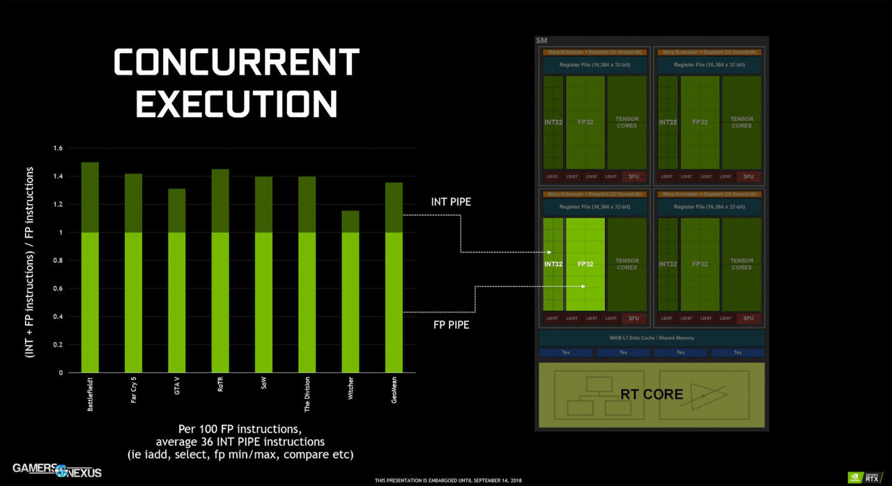
With Pascal SM, integer instruction stalls floating point instruction issues. Turing SM splits integer and floating point data-types into two different paths.

RTX 2060 has 6.5 TFLOPS FP32 with 6.5 TIOPS INT32, hence it's total programmable compute operation is 13 TOPS not including fix function Tensor and TX cores.

AMD's CU can mix FP and INT data-types without penalty.

Without factoring Tensor and RT cores, RTX 2080 Ti's raster power is an evolution over GTX 1080 Ti which still sports similar six GPC (six geometry-raster engines) and 88 ROPS which includes improvements such as higher clock speed, separate integer path, rapid pack math(nearly useless atm) and larger 6 MB L2 cache.

Turing didn't overcome 8 ROPS per 32 bit memory channel limits from Pascal architecture while AMD's NAVI is expected to catch up with it's 8 ROPS per 32 bit memory channel with GDDR6.

VII with 331 mm^2 size has similar transistor count is similar to RTX 2080 with 545 mm^2 size. VII's quad stack HBM v2 at 1000Mhz is expensive.
Avatar image for Shewgenja
Shewgenja

21456

Forum Posts

0

Wiki Points

0

Followers

Reviews: 1

User Lists: 0

#52 Shewgenja
Member since 2009 • 21456 Posts

8k/60 is a flatly unrealistic goal for 9th gen AAA console games. PS5 Pro will likely clean up performance for 8k/30 titles if we are lucky.

Avatar image for crimson_v
Crimson_V

166

Forum Posts

0

Wiki Points

0

Followers

Reviews: 0

User Lists: 5

#53  Edited By Crimson_V
Member since 2014 • 166 Posts

@ronvalencia said:
@crimson_v said:
@boxrekt said:
@rmpumper said:

PS5 wont even do 4K60, genius.

I was going to come in and inform the TC that he was asking for a PC that's doing something that PS5 will absolutely not do, but then I saw your post.

No, PS4 will not do native 8k 60fps in any form. However if you don't think PS5 will do 4k60 you might be more delusional than the TC.

PS5 will absolutely do 4k60 native for the majority of games, hell the X offers 4k 30 for many games now and 1 or 2 4k60 titles.

You'd have to be an idiot to think that PS4 wouldn't be able to do 4k60 when Sony are specifically designing PS5 to do that, but I guess you investing $800 - $1500 on you current PC just to get that has you butthurt and damage controlling. Poor guy.

Also TC, PS5 is going to be $500 not $399. I guess it's fair to say you can this guy are equally delusional.

You need to look more into tech before you go off on an idiotic rant, xbox one x hardly offers native 4k 30fps mostly just on simple indie games the rest is just checkerboarding and other forms of up-scaling.

Currently the best consumer gpu is the RTX 2080 Ti and even that struggles in modern graphically advanced games to keep over 60fps in 4k consistently and lets not even talk about the games that will come out in the next 8 years and that's on a 775mm^2 die, its impossible for a console to have such a large gpu die and even if Navi is denser (which it definitely will be due to it being 7nm) it is unlikely to match the 2080 Ti without having at least that kind of die size.

and why would he be upset even if what you said is future gpu's always perform better then current ones, that's really no surprise to anyone that's into hardware.

There is a reason why consoles are as cheap as they are, because they use bottom of the barrel hardware on everything except the gpu and even that's just mid range in most cases, you get what you pay for.

RTX 2080 Ti is built on 12 nm not 7nm and it has tensor and RT cores wastage.

Turing SM has 64 FP CUDA cores and 64 INT CUDA cores instead of 128 mix FP/INT CUDA cores. The majority of current workloads are FP.

With Pascal SM, integer instruction stalls floating point instruction issues. Turing SM splits integer and floating point data-types into two different paths.

RTX 2060 has 6.5 TFLOPS FP32 with 6.5 TIOPS INT32, hence it's total programmable compute operation is 13 TOPS not including fix function Tensor and TX cores.

AMD's CU can mix FP and INT data-types without penalty.

Without factoring Tensor and RT cores, RTX 2080 Ti's raster power is an evolution over GTX 1080 Ti which still sports similar six GPC (six geometry-raster engines) and 88 ROPS which includes improvements such as higher clock speed, separate integer path, rapid pack math(nearly useless atm) and larger 6 MB L2 cache.

Turing didn't overcome 8 ROPS per 32 bit memory channel limits from Pascal architecture while AMD's NAVI is expected to catch up with it's 8 ROPS per 32 bit memory channel with GDDR6.

VII with 331 mm^2 size has similar transistor count is similar to RTX 2080 with 545 mm^2 size. VII's quad stack HBM v2 at 1000Mhz is expensive.

notice the part where i said "its impossible for a console to have such a large gpu die and even if Navi is denser (which it definitely will be due to it being 7nm)"

so im obviously aware that navi is denser at 7nm then Nvidias Turing arch with 12nm.

I'm in no way an nvidia fanboi but we need to tamper our expectations. Concerning density Vega 64 with 64 CUs at 14nm has a die size of 495 mm² and Vega VII with 60 CUs at 7nm has a die size of 331 mm² (both having almost identical transistor numbers Vega VII having slightly more), Navi is set to still use the GCN arch (obviously there will be improvements to the number of operations it does per clock cycle, people are more so afraid that it will limit the number of CUs/shaders/ROPS but don't quote me on that, it's just an interesting rumor i heard).

So the best case scenario that we can hope for is +30-60% performance in varied workloads (such as gaming) vs Turing at the same die size factoring in architectural improvements and the die shrink, and if we consider the fact that the 2080 Ti can't do (as in reach stable 30fps) 8k in slightly demanding games with its die size of 775 mm², its impossible that next gen consoles with Navi and 200-350 mm² die size (the gpu size that consoles will most probably get) and 15-35% lower then consumer dGPU clock speeds will even come close to being able to do 8k at even 30fps.

Avatar image for ronvalencia
ronvalencia

29612

Forum Posts

0

Wiki Points

0

Followers

Reviews: 1

User Lists: 0

#54  Edited By ronvalencia
Member since 2008 • 29612 Posts

@crimson_v said:
@ronvalencia said:

RTX 2080 Ti is built on 12 nm not 7nm and it has tensor and RT cores wastage.

Turing SM has 64 FP CUDA cores and 64 INT CUDA cores instead of 128 mix FP/INT CUDA cores. The majority of current workloads are FP.

With Pascal SM, integer instruction stalls floating point instruction issues. Turing SM splits integer and floating point data-types into two different paths.

RTX 2060 has 6.5 TFLOPS FP32 with 6.5 TIOPS INT32, hence it's total programmable compute operation is 13 TOPS not including fix function Tensor and TX cores.

AMD's CU can mix FP and INT data-types without penalty.

Without factoring Tensor and RT cores, RTX 2080 Ti's raster power is an evolution over GTX 1080 Ti which still sports similar six GPC (six geometry-raster engines) and 88 ROPS which includes improvements such as higher clock speed, separate integer path, rapid pack math(nearly useless atm) and larger 6 MB L2 cache.

Turing didn't overcome 8 ROPS per 32 bit memory channel limits from Pascal architecture while AMD's NAVI is expected to catch up with it's 8 ROPS per 32 bit memory channel with GDDR6.

VII with 331 mm^2 size has similar transistor count is similar to RTX 2080 with 545 mm^2 size. VII's quad stack HBM v2 at 1000Mhz is expensive.

notice the part where i said "its impossible for a console to have such a large gpu die and even if Navi is denser (which it definitely will be due to it being 7nm)"

so im obviously aware that navi is denser at 7nm then Nvidias Turing arch with 12nm.

I'm in no way an nvidia fanboi but we need to tamper our expectations. Concerning density Vega 64 with 64 CUs at 14nm has a die size of 495 mm² and Vega VII with 60 CUs at 7nm has a die size of 331 mm² (both having almost identical transistor numbers Vega VII having slightly more), Navi is set to still use the GCN arch (obviously there will be improvements to the number of operations it does per clock cycle, people are more so afraid that it will limit the number of CUs/shaders/ROPS but don't quote me on that, it's just an interesting rumor i heard).

So the best case scenario that we can hope for is +30-60% performance in varied workloads (such as gaming) vs Turing at the same die size factoring in architectural improvements and the die shrink, and if we consider the fact that the 2080 Ti can't do (as in reach stable 30fps) 8k in slightly demanding games with its die size of 775 mm², its impossible that next gen consoles with Navi and 200-350 mm² die size (the gpu size that consoles will most probably get) and 15-35% lower then consumer dGPU clock speeds will even come close to being able to do 8k at even 30fps.

TSMC's 1st gen 7nm is not true "7nm" since 2nd gen 7nm+ has further 20 percent density improvements.

https://www.eteknix.com/tsmc-7nm-designs-taped-out-5nm-2019/

7nm+ Node Starts EUV Transition

Due to the refined process, TSMC is expecting about 6-12% reduction in power consumption and 20% increase in density

Applying 7nm+ on VII's fake 7nm 331mm^2 lands on 264 mm^2.

--------

https://hothardware.com/news/analysis-intel-10nm-process-enables-27x-density-over-14nm-nodes

Analysis Says Intel 10nm Process Enables 2.7X Density Over 14nm INTC Nodes

Intel 10 nm is effectively better than 7nm. Intel is careful to avoid "Osborne effect" with their existing product lines, hence Intel hiding their +2X density node.

--------

GCN is not limited by CU count i.e. AMD attached extra CUs on Hawaii 44CU, hence designing Fiji 64 CU. The real problem with GCN is rasterization power exposing the available TFLOPS into graphics operations.

With GDDRx designs, current GCN designs has quad geometry-raster engines with 64 ROPS coupled with 512 bit bus, hence why Polaris 10 has 256bit bus has 32 ROPS.

NVIDIA Pascal/Turing has mastered the following designs

  • 64 ROPS with 256 bit bus and quad geometry-raster engines e.g. GP104 and TU106.
  • 64 ROPS with 256 bit bus and six geometry-raster engines e.g TU104

Mastering "8 ROPS per 32bit bus channel" design enables NVIDIA to build scaled GPU designs like GP102 and TU102 with 96 ROPS with 384 bit bus and six geometry-raster engines. AMD can't do this with their existing GCN design.

NAVI is expected for AMD to master "8 ROPS per 32bit bus channel" design which enable AMD to build GPUs with 64 ROPS and 256 bit bus.

Avatar image for zaryia
Zaryia

21607

Forum Posts

0

Wiki Points

0

Followers

Reviews: 0

User Lists: 0

#55 Zaryia
Member since 2016 • 21607 Posts

PS5 on track to be a distant second place again.

Avatar image for GarGx1
GarGx1

10934

Forum Posts

0

Wiki Points

0

Followers

Reviews: 4

User Lists: 0

#56  Edited By GarGx1
Member since 2011 • 10934 Posts

Hmmm.... Intresdasting

Avatar image for techhog89
Techhog89

5430

Forum Posts

0

Wiki Points

0

Followers

Reviews: 0

User Lists: 0

#57 Techhog89
Member since 2015 • 5430 Posts

Why did this board become so much more stupid over the past week?

Avatar image for Zuon
Zuon

505

Forum Posts

0

Wiki Points

0

Followers

Reviews: 0

User Lists: 0

#58  Edited By Zuon
Member since 2008 • 505 Posts

So, I admit, I couldn't get through all this arguing, but here's why I believe PS5 will aim for a 4K 60FPS target for most games. (Not 8k though, that's silly)

1. Every 3D console generation so far has seen both a graphical fidelity leap and a resolution target increase at the same time. (Excluding post-GC Nintendo)

PS1/N64 = 240p, DC/PS2/GC/XBOX = 480p, Xbox 360/PS3 = 720p, Xbox One/PS4 = 900/1080p, PS4 Pro/XBOX One X = 1440/2160p (4k)

2. The Xbox One X is already targeting 4K 30 and is doing reasonably well at it. It only makes sense that Sony will try to surpass Microsoft with hardware capable of 4K 60 instead. The PS4 Pro needs a successor to compete.

3. PC Hardware already exists for playing modern games at 4k 60FPS at medium-high settings. It is plausible that a next gen console will take advantage of this. And no, I'm not talking GTX 2080ti, moreso 1080ti/AMD VEGA, if a sacrifice needs to be made.

4. Consoles are usually sold at a loss in profits compared to hardware prices, which Sony/Microsoft make up for in game licenses.

Avatar image for MarkoftheSivak
MarkoftheSivak

461

Forum Posts

0

Wiki Points

0

Followers

Reviews: 4

User Lists: 0

#59 MarkoftheSivak
Member since 2010 • 461 Posts

PS5 for $400? Yeah right, I think it's gonna be at least $500 when it releases, maybe even $600.

Avatar image for emgesp
emgesp

7848

Forum Posts

0

Wiki Points

0

Followers

Reviews: 0

User Lists: 0

#60 emgesp
Member since 2004 • 7848 Posts

PS5 isn't going to render AAA games in 8K. Cerny simply said 8K is supported because of the HDMI spec, but devs are not gonna bother.

Avatar image for emgesp
emgesp

7848

Forum Posts

0

Wiki Points

0

Followers

Reviews: 0

User Lists: 0

#61 emgesp
Member since 2004 • 7848 Posts
@rmpumper said:

PS5 wont even do 4K60, genius.

Well thats just straight up wrong. If you mean majority of games, sure, but there will indeed be native 4K 60fps games on both PS5 and XBOX Anaconda. There will definitely be a lot more 60fps games in general compared to current gen thanks to the much better CPU.

Avatar image for crimson_v
Crimson_V

166

Forum Posts

0

Wiki Points

0

Followers

Reviews: 0

User Lists: 5

#62 Crimson_V
Member since 2014 • 166 Posts

@ronvalencia said:
@crimson_v said:
@ronvalencia said:

RTX 2080 Ti is built on 12 nm not 7nm and it has tensor and RT cores wastage.

Turing SM has 64 FP CUDA cores and 64 INT CUDA cores instead of 128 mix FP/INT CUDA cores. The majority of current workloads are FP.

With Pascal SM, integer instruction stalls floating point instruction issues. Turing SM splits integer and floating point data-types into two different paths.

RTX 2060 has 6.5 TFLOPS FP32 with 6.5 TIOPS INT32, hence it's total programmable compute operation is 13 TOPS not including fix function Tensor and TX cores.

AMD's CU can mix FP and INT data-types without penalty.

Without factoring Tensor and RT cores, RTX 2080 Ti's raster power is an evolution over GTX 1080 Ti which still sports similar six GPC (six geometry-raster engines) and 88 ROPS which includes improvements such as higher clock speed, separate integer path, rapid pack math(nearly useless atm) and larger 6 MB L2 cache.

Turing didn't overcome 8 ROPS per 32 bit memory channel limits from Pascal architecture while AMD's NAVI is expected to catch up with it's 8 ROPS per 32 bit memory channel with GDDR6.

VII with 331 mm^2 size has similar transistor count is similar to RTX 2080 with 545 mm^2 size. VII's quad stack HBM v2 at 1000Mhz is expensive.

notice the part where i said "its impossible for a console to have such a large gpu die and even if Navi is denser (which it definitely will be due to it being 7nm)"

so im obviously aware that navi is denser at 7nm then Nvidias Turing arch with 12nm.

I'm in no way an nvidia fanboi but we need to tamper our expectations. Concerning density Vega 64 with 64 CUs at 14nm has a die size of 495 mm² and Vega VII with 60 CUs at 7nm has a die size of 331 mm² (both having almost identical transistor numbers Vega VII having slightly more), Navi is set to still use the GCN arch (obviously there will be improvements to the number of operations it does per clock cycle, people are more so afraid that it will limit the number of CUs/shaders/ROPS but don't quote me on that, it's just an interesting rumor i heard).

So the best case scenario that we can hope for is +30-60% performance in varied workloads (such as gaming) vs Turing at the same die size factoring in architectural improvements and the die shrink, and if we consider the fact that the 2080 Ti can't do (as in reach stable 30fps) 8k in slightly demanding games with its die size of 775 mm², its impossible that next gen consoles with Navi and 200-350 mm² die size (the gpu size that consoles will most probably get) and 15-35% lower then consumer dGPU clock speeds will even come close to being able to do 8k at even 30fps.

TSMC's 1st gen 7nm is not true "7nm" since 2nd gen 7nm+ has further 20 percent density improvements.

https://www.eteknix.com/tsmc-7nm-designs-taped-out-5nm-2019/

7nm+ Node Starts EUV Transition

Due to the refined process, TSMC is expecting about 6-12% reduction in power consumption and 20% increase in density

Applying 7nm+ on VII's fake 7nm 331mm^2 lands on 264 mm^2.

--------

https://hothardware.com/news/analysis-intel-10nm-process-enables-27x-density-over-14nm-nodes

Analysis Says Intel 10nm Process Enables 2.7X Density Over 14nm INTC Nodes

Intel 10 nm is effectively better than 7nm. Intel is careful to avoid "Osborne effect" with their existing product lines, hence Intel hiding their +2X density node.

--------

GCN is not limited by CU count i.e. AMD attached extra CUs on Hawaii 44CU, hence designing Fiji 64 CU. The real problem with GCN is rasterization power exposing the available TFLOPS into graphics operations.

With GDDRx designs, current GCN designs has quad geometry-raster engines with 64 ROPS coupled with 512 bit bus, hence why Polaris 10 has 256bit bus has 32 ROPS.

NVIDIA Pascal/Turing has mastered the following designs

  • 64 ROPS with 256 bit bus and quad geometry-raster engines e.g. GP104 and TU106.
  • 64 ROPS with 256 bit bus and six geometry-raster engines e.g TU104

Mastering "8 ROPS per 32bit bus channel" design enables NVIDIA to build scaled GPU designs like GP102 and TU102 with 96 ROPS with 384 bit bus and six geometry-raster engines. AMD can't do this with their existing GCN design.

NAVI is expected for AMD to master "8 ROPS per 32bit bus channel" design which enable AMD to build GPUs with 64 ROPS and 256 bit bus.

if 7nm+ will be 20% denser that's insane, is this based on the DigiTimes report? (would be really cool if that's true)

as far as i remember Zen2 and Navi is expected to come out back to back on regular non-EUV 7nm so that's the one consoles will most likely use too.

They were definitely behind in terms of pixel throughput so more ROPS will definitely help, i'm also hoping they increase the number of geometry engines per CU so that they catch up on tessalation too.

I'm not quite sure how much better (denser?) intel's 10nm is:

https://www.semiwiki.com/forum/attachments/content/attachments/20527d1507074126-7nm-comparisons.jpg

Avatar image for blaznwiipspman1
blaznwiipspman1

16538

Forum Posts

0

Wiki Points

0

Followers

Reviews: 0

User Lists: 0

#63 blaznwiipspman1
Member since 2007 • 16538 Posts

I remember Linus did a video of a PC doing 16k in a couple of games. He hooked up a 4 x 4 array of 4k gaming monitors so 16 total at 4k res each. The PC was powered with 4 of the highest end gpus on the market at the time, I believe 4 x Quadro p5000 graphics cards in SLI. Each graphics card came with 16gb vram, so a total of 64gb video memory, they needed that much memory just to deal with the amount of pixels rendered. This video was shot more than an year ago also. He could only run Minecraft and tomb raider. Tomb raider ran at like 3fps.

So basically, it's definitely possible to do 8k gaming, that's 4 times less intensive as 16k gaming but you will need graphics card with at least 10gb of video memory to make it work in the first place. Then you will need to find a tv that renders 8k resolution or hook up 2 x 2 array of 4k monitors/tvs. There is no monitor or tv on the market capable of rendering so many pixels, though this will probably change in the next 5 years.

Avatar image for ronvalencia
ronvalencia

29612

Forum Posts

0

Wiki Points

0

Followers

Reviews: 1

User Lists: 0

#64  Edited By ronvalencia
Member since 2008 • 29612 Posts

@crimson_v said:

if 7nm+ will be 20% denser that's insane, is this based on the DigiTimes report? (would be really cool if that's true)

as far as i remember Zen2 and Navi is expected to come out back to back on regular non-EUV 7nm so that's the one consoles will most likely use too.

They were definitely behind in terms of pixel throughput so more ROPS will definitely help, i'm also hoping they increase the number of geometry engines per CU so that they catch up on tessalation too.

I'm not quite sure how much better (denser?) intel's 10nm is:

https://www.semiwiki.com/forum/attachments/content/attachments/20527d1507074126-7nm-comparisons.jpg

https://www.reddit.com/r/PS5/comments/bhabap/well_here_we_go/

So as we all know, the PS5 was "announced" last week. Since then there's been wild speculation on Reddit, Resetera, EuroGamer etc about the power of Sony's Next Generation Console.

Well, a close friend of mine was at a Sony meeting due to the nature of his work.

The meeting took place the day after the PS5 article went up. He's sent me some details about what was mentioned at this meeting and has given me the greenlight to say some things that were mentioned:

8 core Zen 2, clocked at 3.2Ghz.

Custom Navi GPU, 56CU, 1.8Ghz, 12.9TF. RT is hardware based, co engineered by AMD and Sony. (They believe the RT hardware is the basis for the rumour that Navi was built for Sony)

24GB RAM (Type or bandwidth wasn't mentioned)

Custom embeded Solid State solution paired with HDD.

No mention of PSVR 2. At all.

PS4 native backwards compatibility, Boost mode being worked on. No mention of enhanced titles. PS3 BC will stay as part of PS Now for the foreseeable future.

It may not as powerful as some think, Sony say they want a balanced machine that's powerful with limited potential for bottlenecks. My friend also said Sony as of recently wants to position itself as a premium brand and this will be the messaging focus.

That's all I can share and all I know. I'm just a messenger and this is a throwaway account though so I won't be answering questions.

Here is a sneak pic of the Event room: https://imgur.com/jUiU3qc

Sony's Steam box aka PS5. NAVI with 56 CU at 1800 Mhz is like RTX 2070 and RTX 2080 range.

Big Navi 20 replace VII (Vega 20)

Navi 10 replace Polaris 10/20 <----- PS5 SKU level.

Navi 12 replace Polaris 11/12

Sony seems to be determine to avoid another under-powered PS4 Pro repeat. PS5 seems to be PS3 level quality box with AMD IP partner instead of IBM/nVidia IP partners.

Nvidia would have their HDMI 2.1 enabled RTX refresh at similar time period. Incoming GDDR6 are 16000 and 18000 ratings.

Avatar image for ronvalencia
ronvalencia

29612

Forum Posts

0

Wiki Points

0

Followers

Reviews: 1

User Lists: 0

#65  Edited By ronvalencia
Member since 2008 • 29612 Posts

@crimson_v said:

if 7nm+ will be 20% denser that's insane, is this based on the DigiTimes report? (would be really cool if that's true)

as far as i remember Zen2 and Navi is expected to come out back to back on regular non-EUV 7nm so that's the one consoles will most likely use too.

They were definitely behind in terms of pixel throughput so more ROPS will definitely help, i'm also hoping they increase the number of geometry engines per CU so that they catch up on tessalation too.

I'm not quite sure how much better (denser?) intel's 10nm is:

https://www.semiwiki.com/forum/attachments/content/attachments/20527d1507074126-7nm-comparisons.jpg

AMD's Vega era quad geometry-raster engines are like Pascal/Turing with quad GPC counterparts.

GPUs like RTX 2080, GTX 1080 Ti and RTX 2080 Ti has six GPCs, hence no-brainer on NVIDIA's apparent geometry-raster superiority.

With NAVI's 8 ROPS per 32 bit bus channel design, AMD could scale to

8 geometry-raster engines with 128 ROPS as the next R9-290X style 512 bit bus PCB replacement. Eight lanes Shader Engines.

6 geometry-raster engines with 96 ROPS as the next R9-280X style 384 bit bus PCB replacement. Six lanes Shader Engines.

----

4 geometry-raster engines with 64 ROPS is the current four lane Shader Engines design limit.